Image Sensor and Method for Manufacturing the Same

a technology of image sensor and manufacturing method, which is applied in the field of image sensor, can solve problems such as difficulties in optimizing the manufacturing process, and achieve the effects of improving resolution and sensitivity, reducing manufacturing costs, and reducing manufacturing costs

Inactive Publication Date: 2008-11-20
DONGBU HITEK CO LTD
View PDF8 Cites 57 Cited by
  • Summary
  • Abstract
  • Description
  • Claims
  • Application Information

AI Technical Summary

Benefits of technology

[0008]An embodiment of the present invention provides an image sensor including a photodiode capable of raising quantum efficiency and a method for manufacturing the same.
[0009]According to an embodiment, an image sensor and a method for manufacturing the same are provided capable of improving resolution and sensitivity.
[0010]Embodiments of the present invention employ a vertically arranged photodiode. Further embodiments can inhibit certain defects from being formed in the photodiode.

Problems solved by technology

Furthers the CMOS image sensor according to the related art has difficulties in optimizing the manufacturing process when the photodiodes and the transistors are simultaneously manufactured.

Method used


Image

  • Image Sensor and Method for Manufacturing the Same
  • Image Sensor and Method for Manufacturing the Same
  • Image Sensor and Method for Manufacturing the Same

Examples


second embodiment

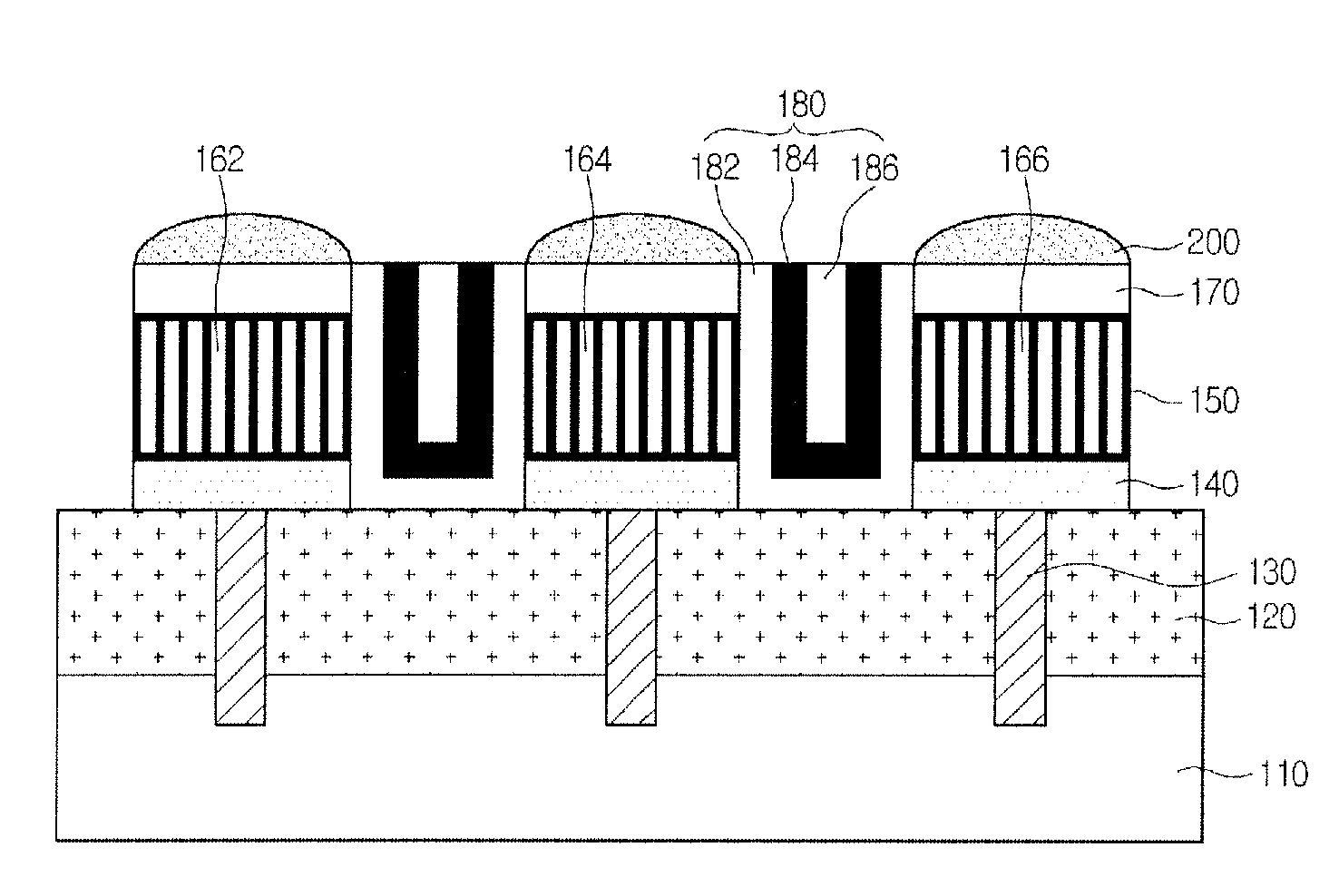
[0056]FIG. 3 is a cross-sectional view showing an image sensor according to a

[0057]The image sensor according to the second embodiment can employ the basic characteristics of the image sensor according to the embodiments described above.

[0058]However, in the image sensor according to the second embodiment, the carbon nanotubes 150a can be doped with a second conductive-type material. According to certain embodiments, a first conductive-type conductive layer 210 can be formed on the lower interconnection 140, and the second conductive-type carbon nanotubes 150a can be formed on the first conducive-type conductive layer 210.

[0059]In one embodiment, the first conductive-type conductive layer 210 can include n-doped amorphous silicon. However, embodiments are not limited thereto.

[0060]According to certain embodiments, the first conductive-type conductive layer 210 includes, but is not limited to a-Si:H, a-SiGe:H, a-SiC, a-SiN:H, or a-SiO:H obtained by adding germanium, carbon, nitrogen,...

third embodiment

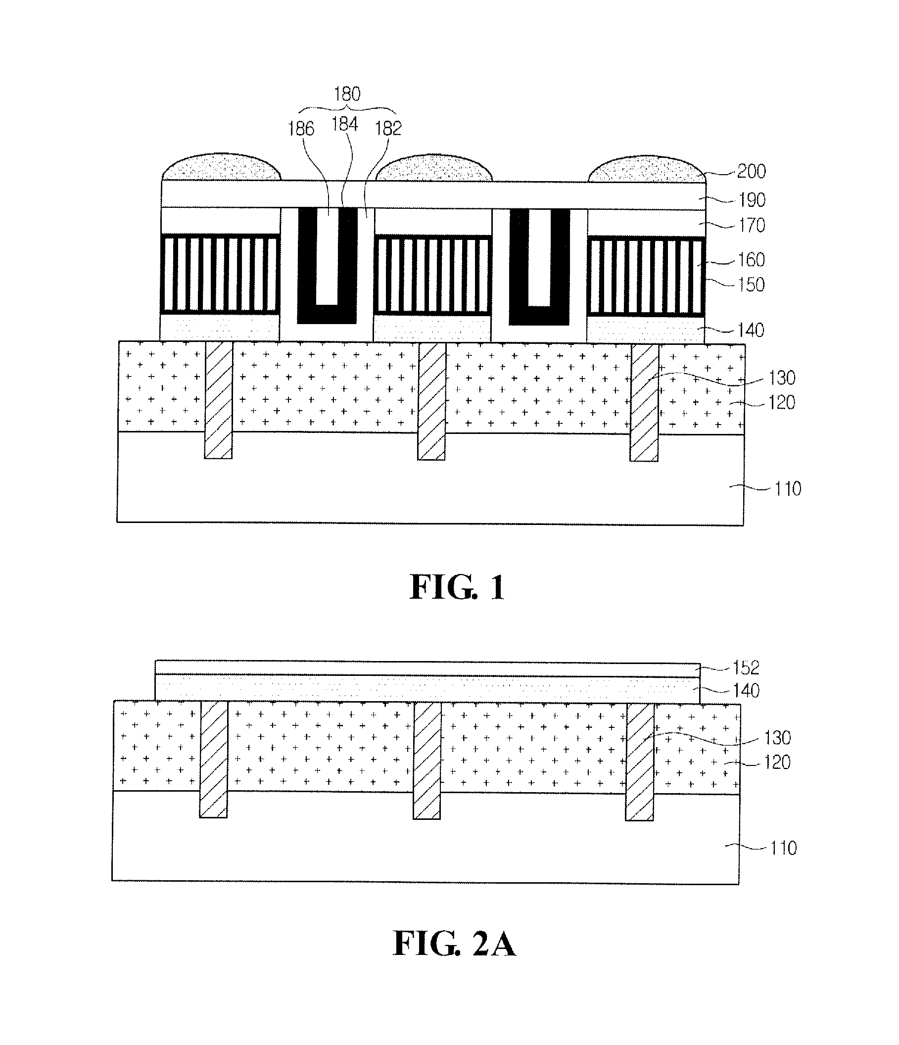
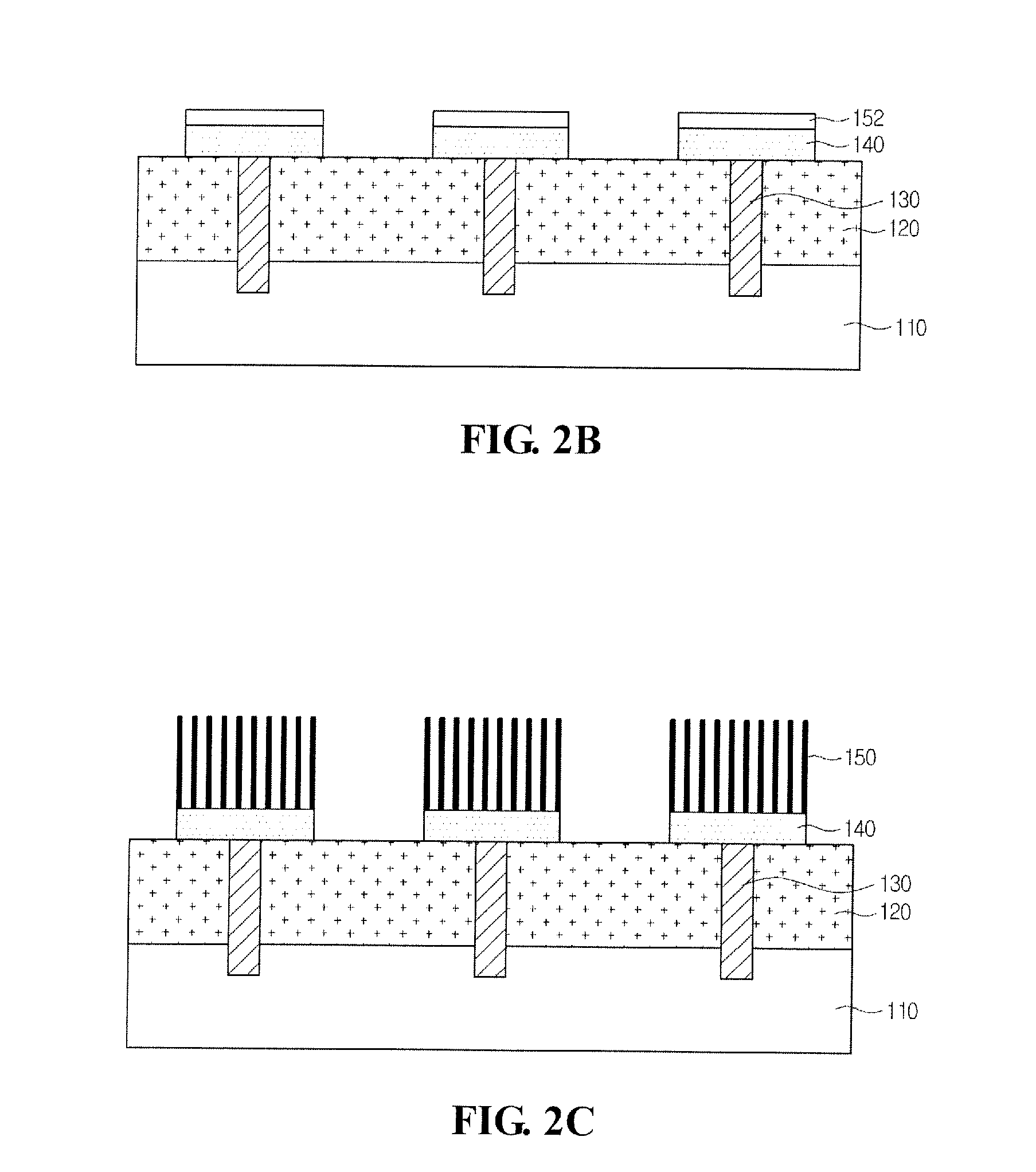
[0063]FIG. 4 is a cross-sectional view showing an image sensor according to a

[0064]The image sensor according to the third embodiment can employ the basic characteristics of the image sensors according to the above described embodiments.

[0065]However, the image sensor according to the third embodiment can further include an intrinsic layer 220 formed on the first conductive-type conductive layer 210. Second conductive-type carbon nanotubes 150a can be formed on the intrinsic layer 220.

[0066]In one embodiment, the intrinsic layer 220 can be formed by using amorphous silicon. The intrinsic layer 220 can be formed through CVD, such as PECVD. For example, the intrinsic layer 220 can be formed using amorphous silicon through the PECVD process by applying SiH4.

fourth embodiment

[0067]FIG. 5 is a cross-sectional view showing an image sensor according to a

[0068]The image sensor according to the fourth embodiment can employ basic characteristics of image sensors according to the above described embodiments.

[0069]However, the image sensor according to the fourth embodiment includes first conductive-type carbon nanotubes 150b. In an embodiment, a second conductive-type conductive layer 230 can be formed on the first conductive-type carbon nanotubes 150b. In a further embodiment, the image sensor can include an intrinsic layer 220 formed on the first conductive-type carbon nanotubes 150b, and the second conductive-type conductive layer 230 is formed on the intrinsic layer 220.

[0070]In one embodiment, the carbon nanotubes 150b can be doped with an N type material. However, embodiments are not limited thereto.

[0071]The second conductive-type conductive layer 230 can be formed subsequently to the process of forming the intrinsic layer 220. In one embodiment, the se...


PUM

PropertyMeasurementUnit
temperatureaaaaaaaaaa
conductiveaaaaaaaaaa
conductive-type conductiveaaaaaaaaaa

Abstract

An image sensor and a method for manufacturing the same are provided. The image sensor can include transistor circuitry on a substrate, and a photodiode arranged above the transistor circuitry. The photodiode can include carbon nanotubes and a conductive polymer layer on the carbon nanotubes. A transparent conducting electrode can be provided on the carbon nanotubes.

Description

CROSS-REFERENCE TO RELATED APPLICATION[0001]The present application claims the benefit under 35 U.S.C. §119 of Korean Patent Application No. 10-2007-0047589, filed May 16, 2007, which is hereby incorporated by reference in its entirety.BACKGROUND[0002]A typical CMOS image sensor includes a photodiode area for receiving an optical signal to convert the optical signal into an electrical signal, and a transistor area for processing the electrical signal.[0003]According to the related art, the photodiodes and transistors are horizontally disposed in the CMOS image sensor.[0004]In other words, in the CMOS image sensor according to the related art, the photodiodes and the transistors are positioned on a substrate such that they are horizontally adjacent to each other. Accordingly, additional areas are required for the photodiodes. For this reason, a fill factor area may be reduced, and resolution may be restricted.[0005]Furthers the CMOS image sensor according to the related art has diffi...

Claims


Application Information

Patent Timeline
Patent Type & Authority Applications(United States)
IPC IPC(8): H01L27/146H01L31/18
CPCB82Y10/00H01L27/14609H01L27/307H01L51/0048H01L51/424H01L51/444Y02E10/549Y02P70/50H10K39/32H10K85/221H10K30/20H10K30/821H01L27/146B82Y20/00
Inventor SHIM, CHEON MAN
Owner DONGBU HITEK CO LTD
Why Eureka
Try Eureka