Solid state photomultiplier using buried P-N junction

a photomultiplier and solid-state technology, applied in the direction of diodes, semiconductor devices, radiation control devices, etc., can solve the problems of apds having performance limitations, limited pmts, and high voltage,

Active Publication Date: 2017-08-08
RADIATION MONITORING DEVICES
View PDF2 Cites 33 Cited by
  • Summary
  • Abstract
  • Description
  • Claims
  • Application Information

AI Technical Summary

Problems solved by technology

PMTs are limited in that they are bulky, require high voltage, and are susceptible to large magnetic fields and helium, for example.
The APDs do, however, have some performance limitations.
In particular, the gain of most APD designs is not very high.
Another disadvantage is that the temporal response of most APD designs is also not as fast as that of high-end PMTs.
The use of commercial CMOS processfacilitates the integration of circuit components, and theuse of an available multi-user service substantiallyreduces the development cost and time.
The second significant noise term arises from statistical fluctuations in the optical cross talk between pixels in the SSPM.
The Geiger discharge from the GPD pixels in the SSPM produces hot carrier emission of photons from the diode, which may cause cross talk between pixels.
The third source of noise in the SSPM arises from the statistical fluctuations associated with after pulsing.
Since there is a probability associated with the occurrence of an after pulse, these pulses add to the parallel noise of the device when integrating the signal.

Method used


Image

  • Solid state photomultiplier using buried P-N junction
  • Solid state photomultiplier using buried P-N junction
  • Solid state photomultiplier using buried P-N junction

Examples


Embodiment Construction

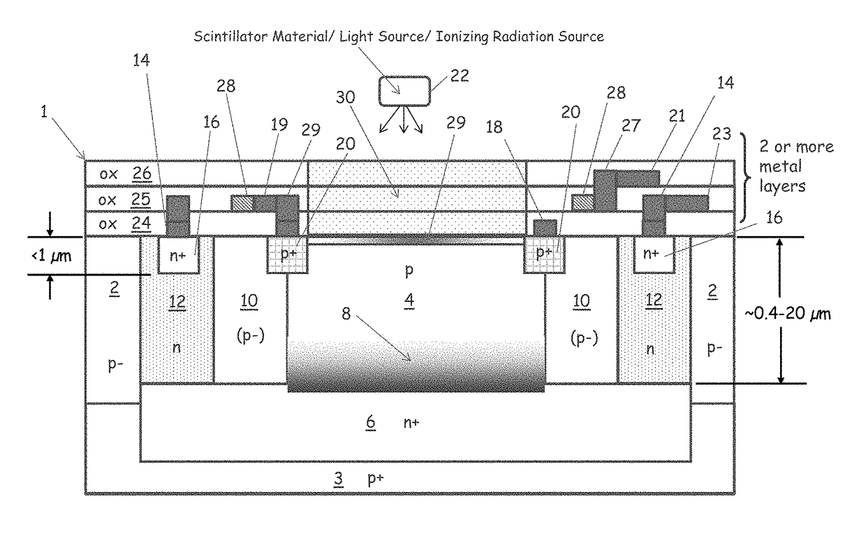
[0021]Described herein is a photodiode having a buried semiconductor layer of a high doping concentration, according to some embodiments. The photodiode may be operated as a Geiger photodiode, such that it is reverse biased above its breakdown voltage. An array of such photodiodes can be used to form a solid state photomultiplier (SSPM) that detects electromagnetic radiation. A radiation detector can be produced that includes a scintillator material and a SSPM. The SSPM can detect light produced by the scintillator material in response to incident radiation, including ionizing and non-ionizing radiation. The photodiode described herein may be used for photodetection or for detection of any phenomenon that may generate an electron-hole pair in the diode that may cause the diode to undergo a self-sustained avalanche.

[0022]FIG. 1 shows a cross section of a photodiode structure 1 having a buried layer, according to some embodiments. Also shown in FIG. 1 is a material 22 that may produce...


PUM


Abstract

A device that detects single optical and radiation events and that provides improved blue detection efficiency and lower dark currents than prior silicon SSPM devices. The sensing element of the devices is a photodiode that may be used to provide single photon detection through the process of generating a self-sustained avalanche. The type of diode is called a Geiger photodiode or signal photon-counting avalanche diode. A CMOS photodiode can be fabricated using a “buried” doping layer for the P-N junction, where the high doping concentration and P-N junction is deep beneath the surface, and the doping concentration at the surface of the diode may be low. The use of a buried layer with a high doping concentration compared to the near surface layer of the primary P-N junction allows for the electric field of the depletion region to extend up near the surface of the diode. With a low doping concentration through the bulk of the diode, the induced bulk defects are limited, which may reduce the dark current. The resulting structure provides a diode with improved quantum efficiency and dark current.

Description

CROSS-REFERENCE TO RELATED APPLICATIONS[0001]This application is a continuation of U.S. application Ser. No. 13 / 656,089, filed Oct. 19, 2012, which claims priority under 35 U.S.C. 119(e) to U.S. Provisional Application No. 61 / 549,958, filed Oct. 21, 2011, which are hereby incorporated by reference in their entirety.BACKGROUND[0002]1. Technical Field[0003]Described herein is a photodiode having a buried P-N junction. The photodiode may be used in a solid-state photomultiplier that can detect optical or radiation events.[0004]2. Discussion of the Related Art[0005]Photomultiplier tubes (PMTs) are a standard technology for detecting small light pulses. The photomultiplier tube is a vacuum tube technology that uses a photocathode, dynodes, and an anode. PMTs provide excellent performance characteristics in that they have a large gain (˜106) and have a good quantum efficiency over the spectral range determined by the photocathode material. PMTs are limited in that they are bulky, require ...

Claims


Application Information

Patent Timeline
Patent Type & Authority Patents(United States)
IPC IPC(8): H01L31/00H01L27/144H01L27/06H01L31/02H01L27/146H01L31/107
CPCH01L31/1075H01L31/02027H01L27/0629H01L27/1446H01L27/14609H01L31/107H01L31/022408
Inventor JOHNSON, ERIK BJORNCHEN, XIAO JIEWHITNEY, CHADSTAPELS, CHRISTOPHERCHRISTIAN, JAMES F.
Owner RADIATION MONITORING DEVICES
Why Eureka
Try Eureka