Array substrate and color filter substrate of display device and method for manufacturing the same

Active Publication Date: 2013-05-02
BEIJING BOE OPTOELECTRONCIS TECH CO LTD
View PDF7 Cites 6 Cited by
  • Summary
  • Abstract
  • Description
  • Claims
  • Application Information

AI Technical Summary

Benefits of technology

[0006]However, the inventors have noted that: in the above pixel structure, the wide common electrode above the data line still causes transmittance loss at the location of the data line.
[0007]One of the problems to be solved by the present invention is to provide an array substrate and a color filter substrate of a display device and a method for manufacturing the same, for effectively restraining signals over data lines from interfering with modulation by liquid crystal thereon and improving light transmittance.
[0008]An aspect of the present invention provides an array substrate comprising: a base substrate, a gate line disposed on the base substrate, a data line disposed perpendicular to the gate line, and a pixel region defined by the gate line intersecting the data line, in which a thin film transistor, a pixel electrode, and a common electrode w

Problems solved by technology

However, the inventors have noted that: in the above pixel structure, the wide common elec

Method used


Image

  • Array substrate and color filter substrate of display device and method for manufacturing the same
  • Array substrate and color filter substrate of display device and method for manufacturing the same
  • Array substrate and color filter substrate of display device and method for manufacturing the same

Examples


first embodiment

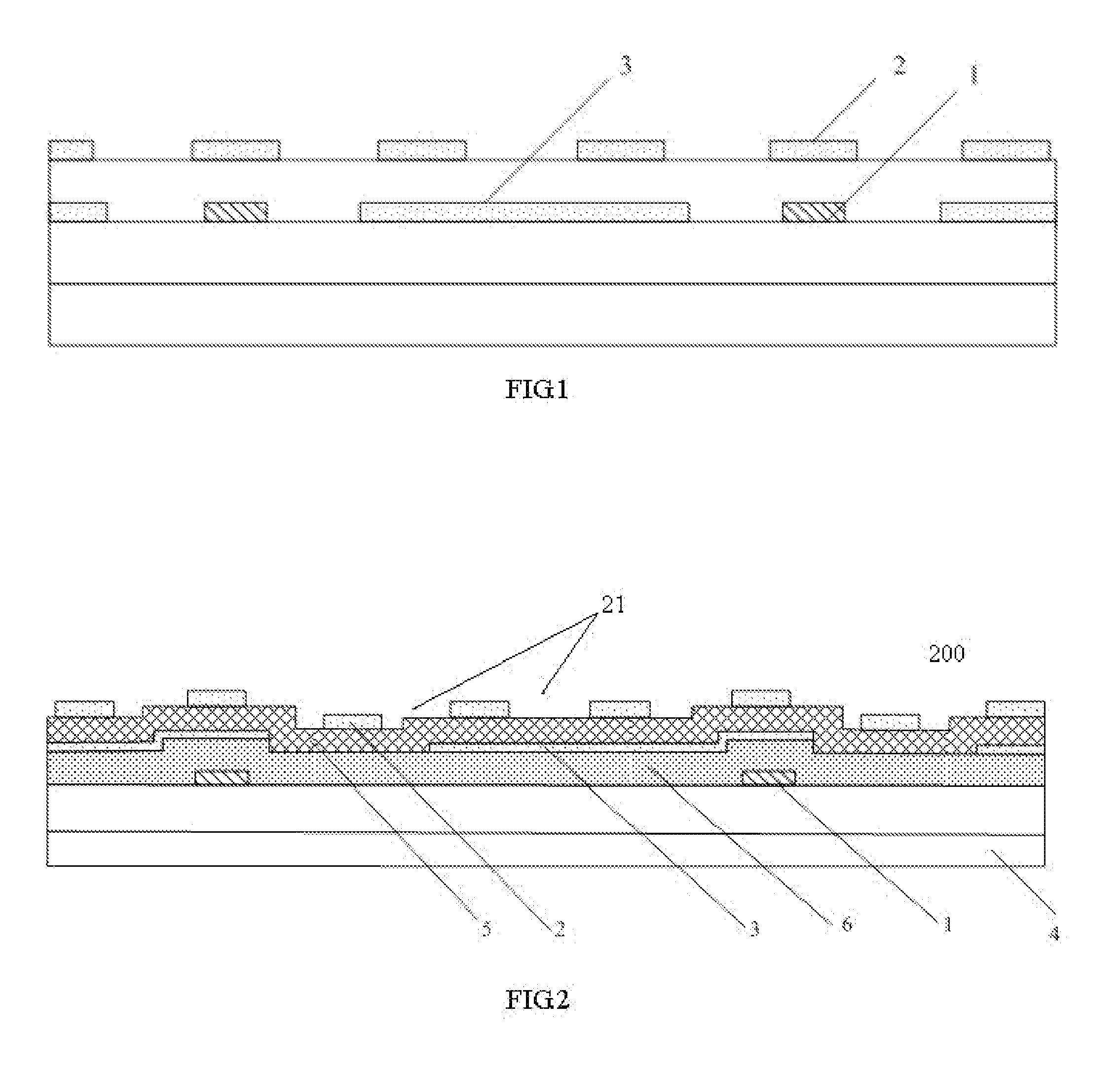
[0030]The first embodiment of the present invention provides an array substrate, as shown in FIG. 2. The array substrate 100 includes a base substrate 4, gate lines (not shown in drawings) disposed on the base substrate 4, and data lines 1 perpendicular to the gate lines. The gate lines intersect the data lines 1 to define a plurality of pixel regions. A thin film transistor (not shown), a pixel electrode 3, and a common electrode 2 for cooperating with the pixel electrode 3 to generate a multi-dimension electric field are disposed in each pixel region. In the embodiment, the pixel electrode 3 is a plate-shaped electrode without slits, and the common electrode 2 is a slit-shaped electrode in which a plurality of slits 21 are formed. A first insulating layer 5 is disposed between the common electrode 2 and the pixel electrode 3. An end of the plate-shaped pixel electrode 3 is located above and covers the data line 1, and a second insulating layer 6 is disposed between a layer of the ...

second embodiment

[0034]The second embodiment is different from the first embodiment in that: the common electrode is a plate-shaped electrode, and the pixel electrode is a slit-shaped electrode; an end of the plate-shaped common electrode is located above and covers the data line, and the second insulating layer is disposed between the common electrode and the data line; the slit-shaped pixel electrode is formed on the common electrode, and the first insulating layer is disposed between the pixel electrode and the common electrode.

[0035]Therefore, in the array substrate of the present embodiment, an end of the common electrode is located above and covers the data line (the pixel electrode is also above the data line), and an insulating layer is disposed between the common electrode and the data line for insulation and protection. In this way, the interference by the data lines with the modulation by the liquid crystal thereon is restrained, the area of the multi-dimension electric field is increased...

third embodiment

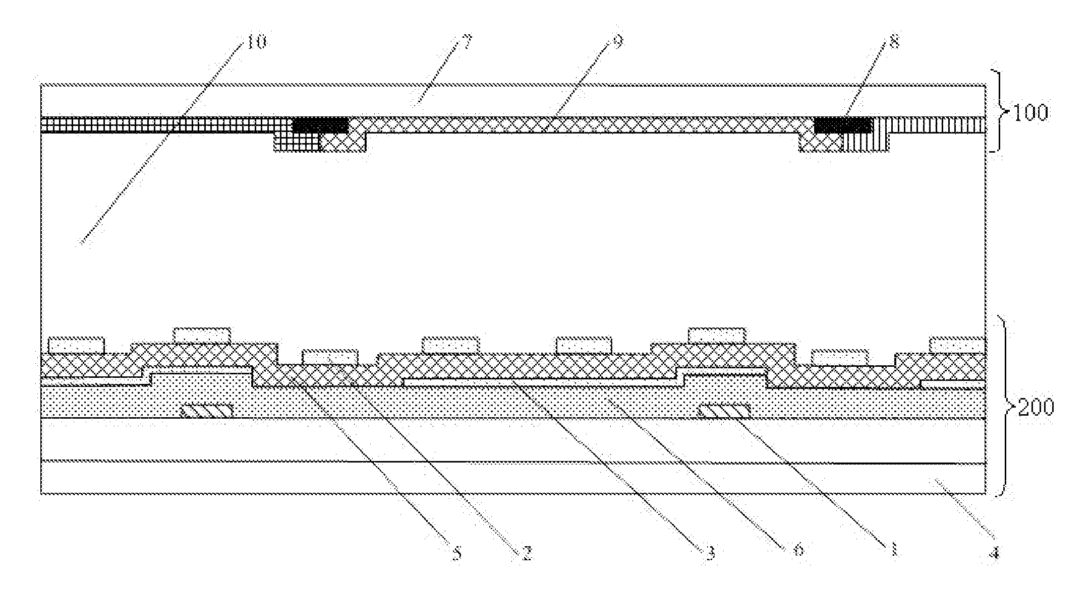
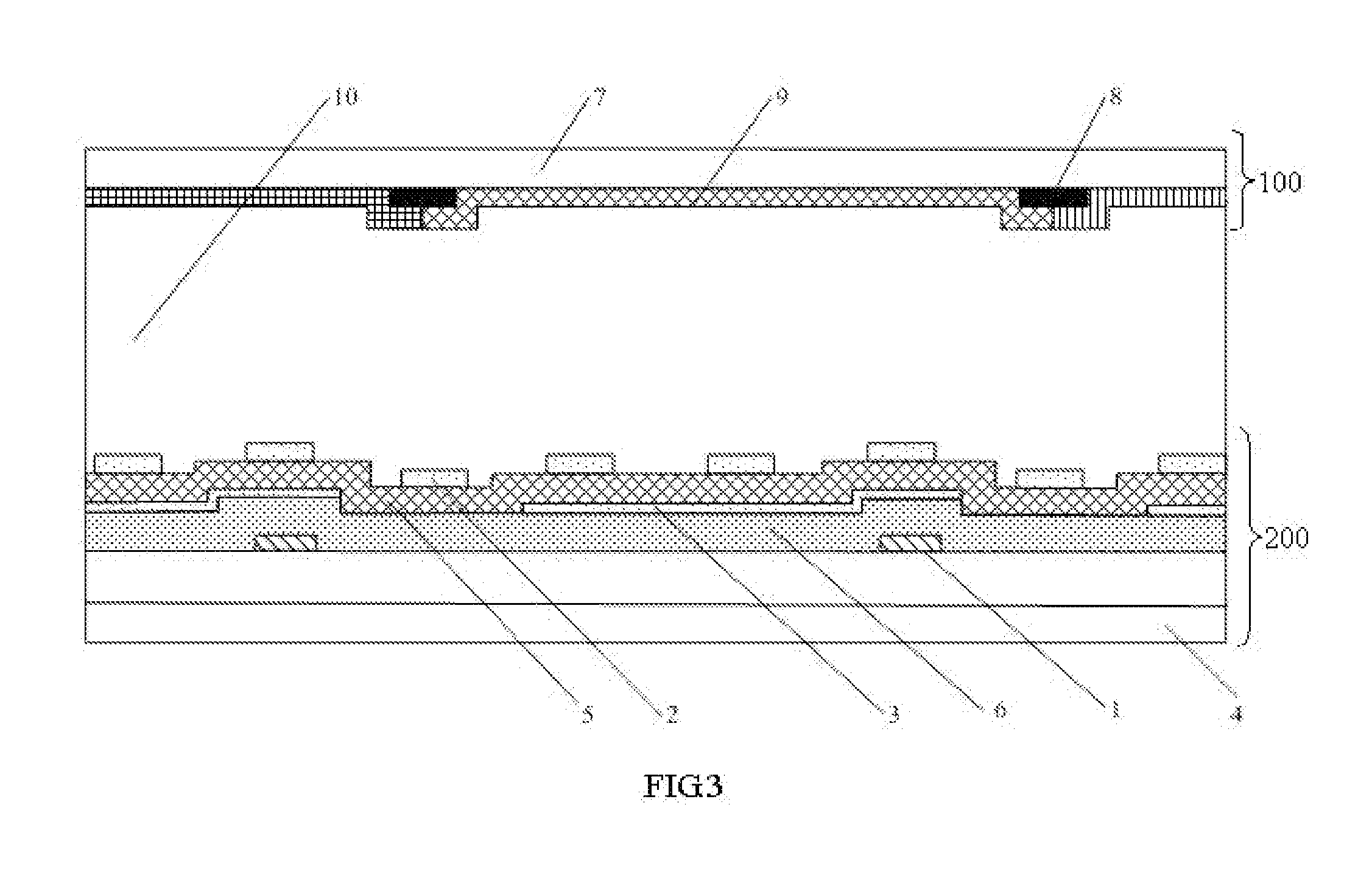
[0036]The embodiment of the present invention also provides a liquid crystal panel. As shown in FIG. 3, a liquid crystal panel according to an example of the embodiment includes a color filter substrate 100, the array substrate 200 of the first embodiment, and a liquid crystal layer 10 between the array substrate 200 and the color filter substrate 100.

[0037]The color filter substrate 100 includes: a base substrate 7, black matrixes 8 formed on the base substrate 7, and color resin sheets 9 formed between the black matrixes 8, the black matrixes 8 are disposed at positions corresponding to gate lines, thin film transistors, and a region without data lines and between adjacent pixels on the array substrate 200. The black matrixes 8 of the color filter substrate define a plurality of sub-pixel regions, each sub-pixel region includes a color resin sheet 9 such as a red, green, and blue resin sheet, and therefore red, green, and blue (RGB) sub-pixels are formed. The sub-pixel regions of ...


PUM


Abstract

Embodiments of the present invention discloses an array substrate of display device and a method for manufacturing the same, which can effectively restrain the interference by the signals over data lines with the modulation conducted by liquid crystal thereon, and improve light transmittance. The array substrate comprises: a pixel region defined by a gate line intersecting a data line. A thin film transistor, a pixel electrode, and a common electrode, which cooperates with the pixel electrode to form a multi-dimension electric field, are disposed in the pixel region. The pixel electrode is a slit-shaped electrode, and the common electrode is a plate-shaped electrode; or the pixel electrode is a plate-shaped electrode, and the common electrode is a slit-shaped electrode. An end of the plate-shaped electrode covers the data line, and a second insulating layer is disposed between a layer of the plate-shaped electrode and a layer of the data line.

Description

TECHNICAL FIELD[0001]Embodiments of present invention relate to an array substrate and a color filter substrate of a liquid crystal display (LCD) and a method for manufacturing the same.BACKGROUND[0002]In flat panel display technology, LCDs have the advantages such as small volume, low power consumption, little radiation, lower costs, etc., and therefore have prevailed in the current flat panel display market.[0003]In an Advanced-Super Dimensional Switching (ADS) technology, a multi-dimensional electric field is formed with both an electric field produced at edges of slit electrodes on the same plane and an electric field produced between a pixel electrode layer and a common electrode layer, so that liquid crystal molecules at all orientations, which are located directly above the electrodes and between the slit electrodes in a liquid crystal cell, can be rotated and aligned, which enhances the work efficiency of planar-oriented liquid crystals and increases light transmittance. The...

Claims


Application Information

Patent Timeline
IPC IPC(8): H01L33/08
CPCG02F1/134309G02F2001/134381G02F1/136286G02F2201/40G02F1/134318G02F1/134372G02F1/1343G02F1/1368
Inventor LI, CHENGDONG, XUECHEN, DONGMU, SUZHEN
Owner BEIJING BOE OPTOELECTRONCIS TECH CO LTD
Why Eureka
Try Eureka