
Touch device and fabrication method thereof
a technology of touch device and fabrication method, which is applied in the field of touch device, can solve the problems of bad appearance of traditional touch device, and achieve the effect of increasing the yield of the touch devi
- Summary
- Abstract
- Description
- Claims
- Application Information
AI Technical Summary
Benefits of technology
Problems solved by technology
Method used
Image

Examples
Embodiment Construction
[0011]In order to make the foregoing objectives, features, and advantages of the present disclosure more comprehensive, several embodiments accompanied with drawings are described in detail below:
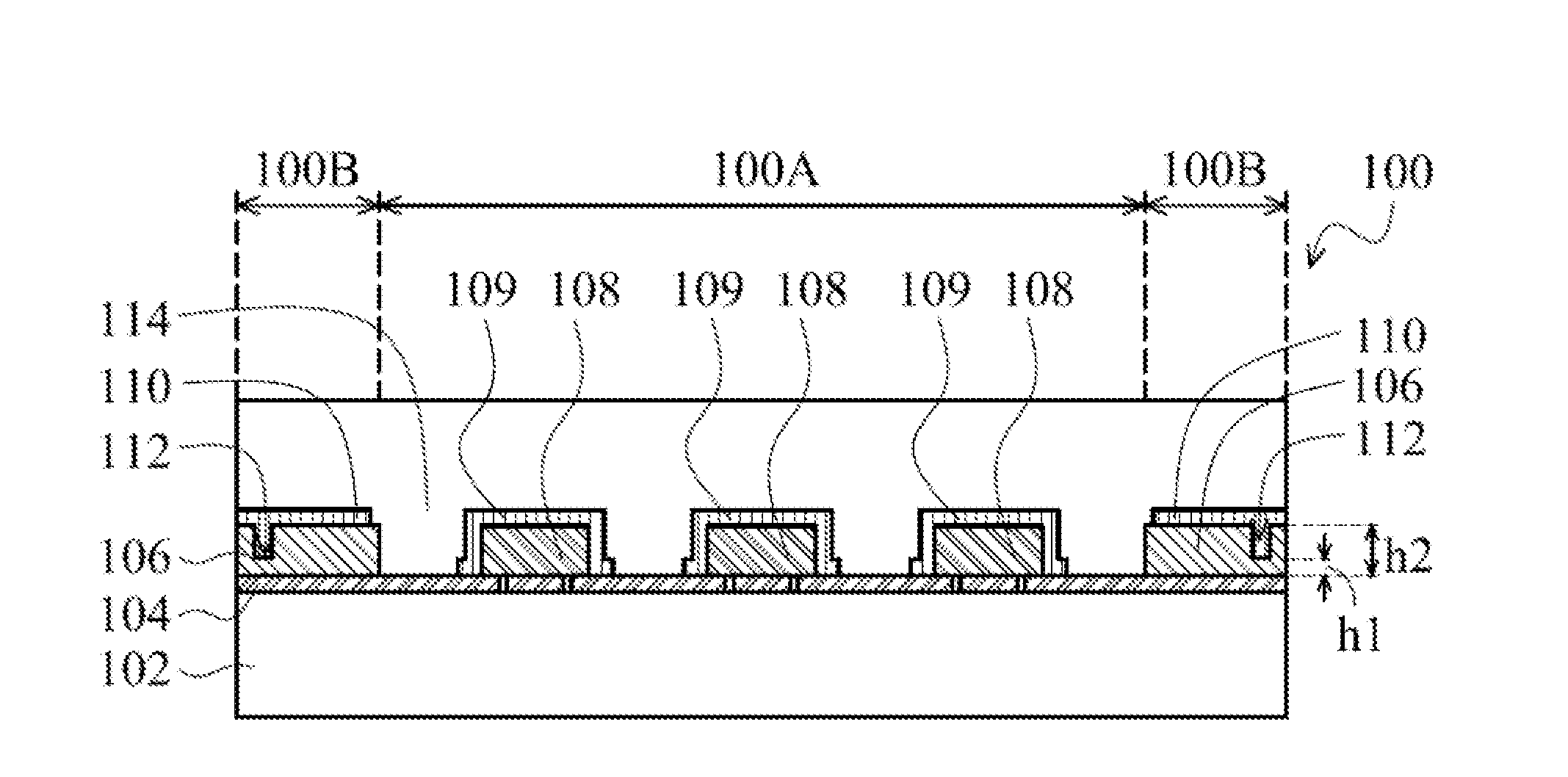
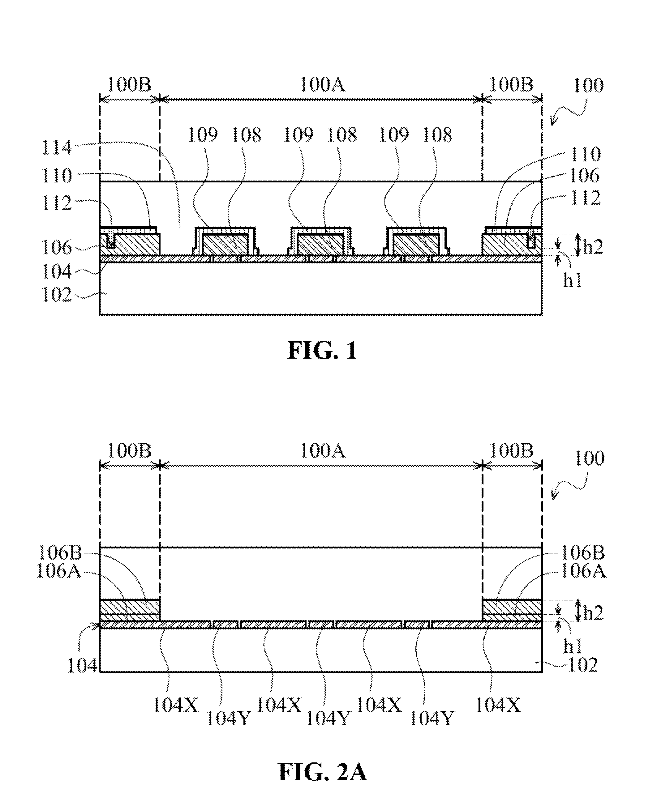
[0012]FIG. 1 shows a section view diagram of a touch device 100 in accordance with an embodiment of the present disclosure. The touch device 100 comprises a capacitive touch device having a sensing area 100A and a peripheral area 100B surrounding the sensing area 100A.
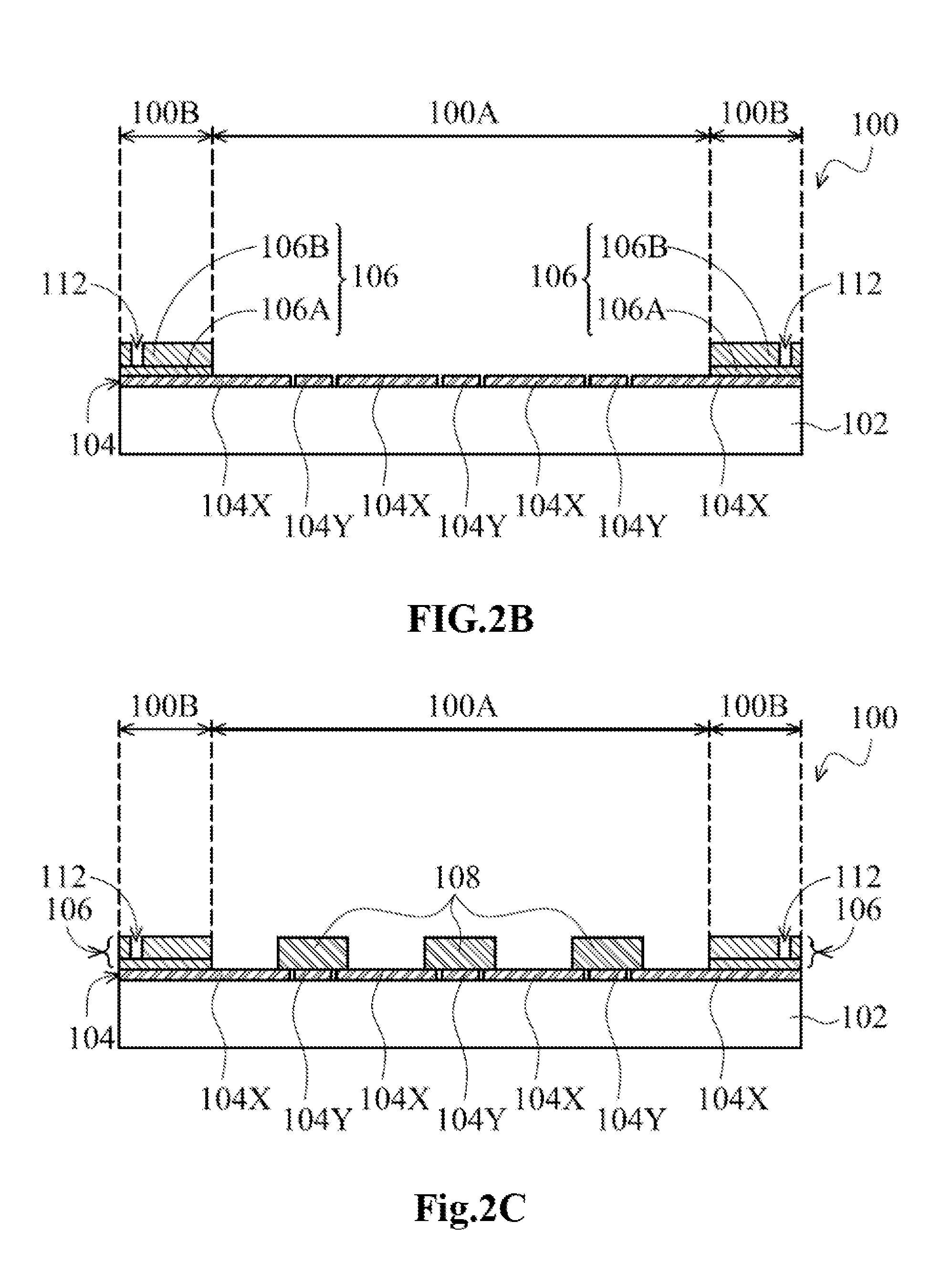
[0013]Touch components of the touch device 100 are disposed on a protective cover 102 (touch on lens), wherein external surface of the protective cover 102 is the touch surface of the touch device 100, and material of the protective cover can be a reinforced glass or any other applicable material. A sensing electrode layer 104 is disposed on the internal surface of the protective cover 102, and material of the sensing electrode layer 104 can be a transparent conductive material such as indium tin oxide (ITO), indium zinc oxide...
PUM
| Property | Measurement | Unit |
|---|---|---|
| longitudinal impedance | aaaaa | aaaaa |
| longitudinal impedance | aaaaa | aaaaa |
| longitudinal impedance | aaaaa | aaaaa |
Abstract
Description
Claims
Application Information