
System and Method for In Situ Monitoring of Top Wafer Thickness in a Stack of Wafers

a technology of in situ monitoring and stacking, which is applied in the direction of measuring devices, instruments, using optical means, etc., can solve the problems of erroneous top wafer thickness measurement of contact probes, blocking of light emitted by the probe, and inability to use contact probes with stacked wafers

Active Publication Date: 2013-05-09
REVASUM INC +1
View PDF2 Cites 5 Cited by
  • Summary
  • Abstract
  • Description
  • Claims
  • Application Information

AI Technical Summary

Benefits of technology

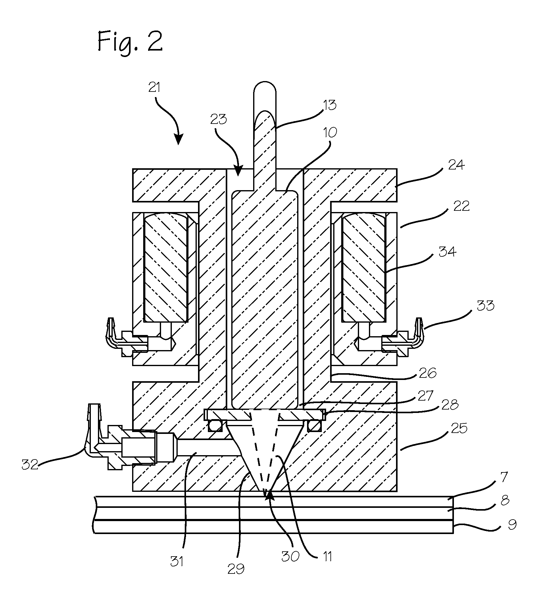
The patent describes a way to position probes over a wafer and suspend them just above it, while using a stream of fluid to carry away any debris that might block the light transmission. This helps to ensure clear and accurate measurements.

Problems solved by technology

Contact probes are not always suitable for use with stacked wafers because they do not provide separate information of the top wafer thickness.
Variations in carrier wafer thickness can lead to erroneous top wafer thickness measurement by the contact probe.
However, during the grinding process, debris builds up on the back surface of the wafer so that the light emitted by the probe is blocked by the debris.

Method used


Image

  • System and Method for In Situ Monitoring of Top Wafer Thickness in a Stack of Wafers
  • System and Method for In Situ Monitoring of Top Wafer Thickness in a Stack of Wafers
  • System and Method for In Situ Monitoring of Top Wafer Thickness in a Stack of Wafers

Examples


Embodiment Construction

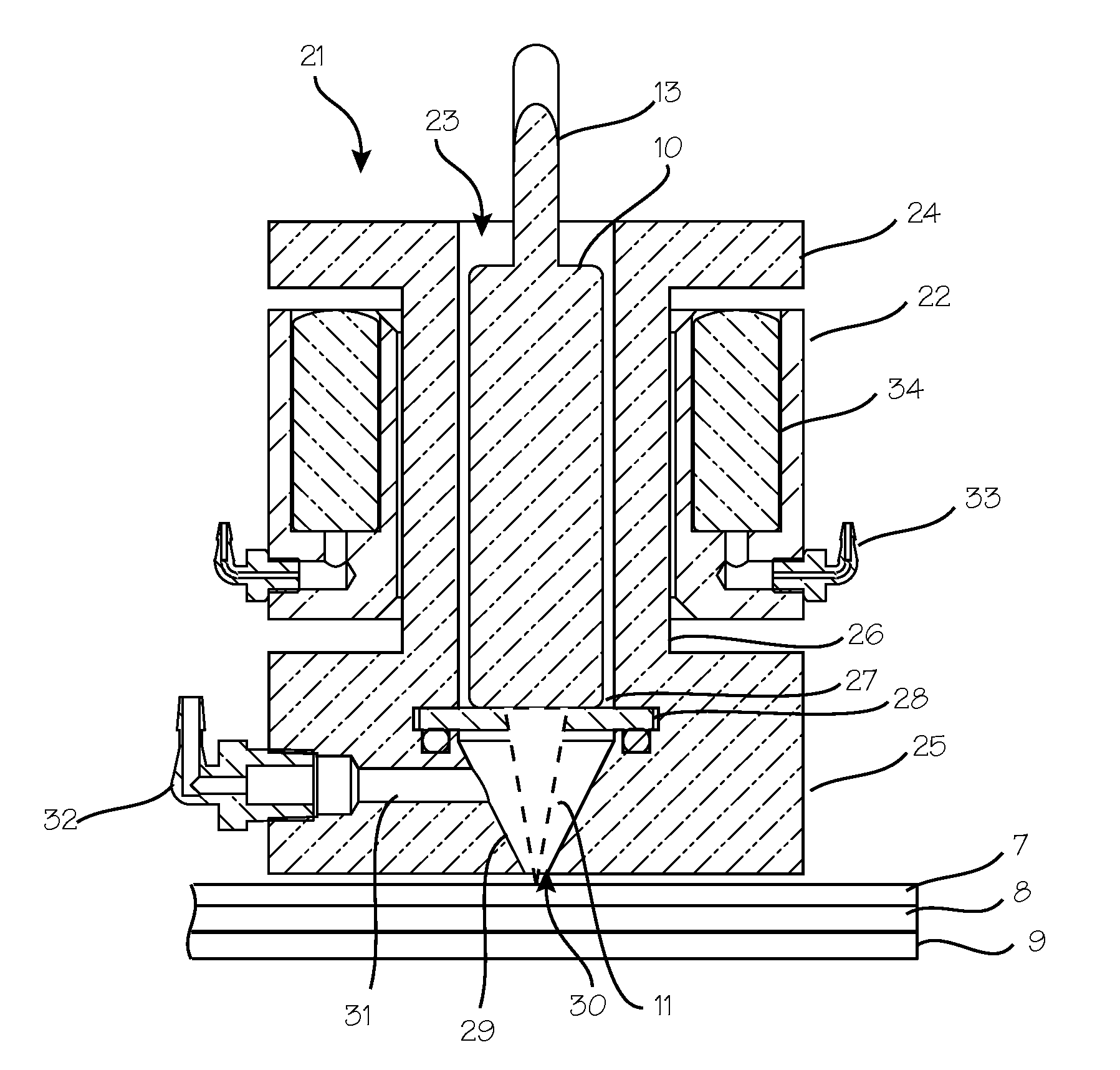
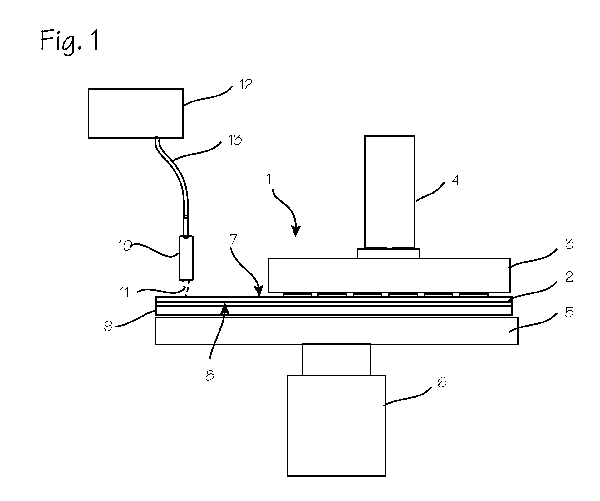
[0010]FIG. 1 illustrates the grinding process and a conventional non-contact probe and wafer in a grinding system 1. A wafer 2 is disposed below a grinding wheel 3. The grinding wheel is supported and rotated by the grinding wheel spindle 4, and the wafer is supported by the wafer holder / chuck 5 which in turn is supported and rotated by the wafer-chuck spindle 6. The wafer being processed may be a stacked wafer which includes a processed wafer with a silicon base layer 7 (and numerous other layers 8 built up upon its “front side”) and a carrier wafer 9 under the processed wafer. During the grinding process, the optical probe system is operated to monitor the thickness of the silicon base layer of the top wafer as it is ground. The probe system includes probe body 10 which transmits light and receives reflected light through the probe light path 11. Light is typically transmitted from a remote light source 12, through optical conduit 13 (fiber optics or waveguide) and optical probe b...


PUM


Abstract

A system for holding non-contact wafer probes over the surface of a wafer which includes a system for flushing the surface of the probe during grinding.

Description

FIELD OF THE INVENTIONS[0001]The inventions described below relate to the field of wafer processing and measurement of wafer thickness.BACKGROUND OF THE INVENTIONS[0002]Recent manufacturing techniques for computer chips require removal of a large portion of the base layer of silicon after the computer chips have been built up on the base layer. To remove the base layer, a wafer with numerous devices built up on the wafer is thinned in a process referred to as backgrinding. Backgrinding is accomplished after the devices are built up, but before the wafer is diced into individual computer chips. The goal of the backgrinding is to reduce the thickness of the base layer of silicon to a predetermined thickness. When the backgrinding process is used to reduce the thickness of the base wafer to such a thin dimension that the wafer is extremely weak, and is subject to easy breakage, the base wafer is sometimes mounted to another full-thickness wafer to provide handling strength. The wafer t...

Claims


Application Information

Patent Timeline
Patent Type & Authority Applications(United States)
IPC IPC(8): G01B11/28
CPCG01B11/0683G01B11/0625
Inventor SCHRAUB, FREDERIC ANTHONYVOGTMANN, MICHAEL R.SMEDLEY, BENJAMIN C.
Owner REVASUM INC
Learn More