Ball grid array to pin grid array conversion

a technology of ball grid array and pin grid array, which is applied in the direction of gas flame welding apparatus, non-electric welding apparatus, electrical apparatus, etc., can solve the problems of limiting or otherwise restricting the ability to use, requiring additional time and tooling to prepare, and cost-effectively different production lines to manufactur

Active Publication Date: 2013-05-23
STMICROELECTRONICS SRL
View PDF1 Cites 11 Cited by
  • Summary
  • Abstract
  • Description
  • Claims
  • Application Information

AI Technical Summary

Benefits of technology

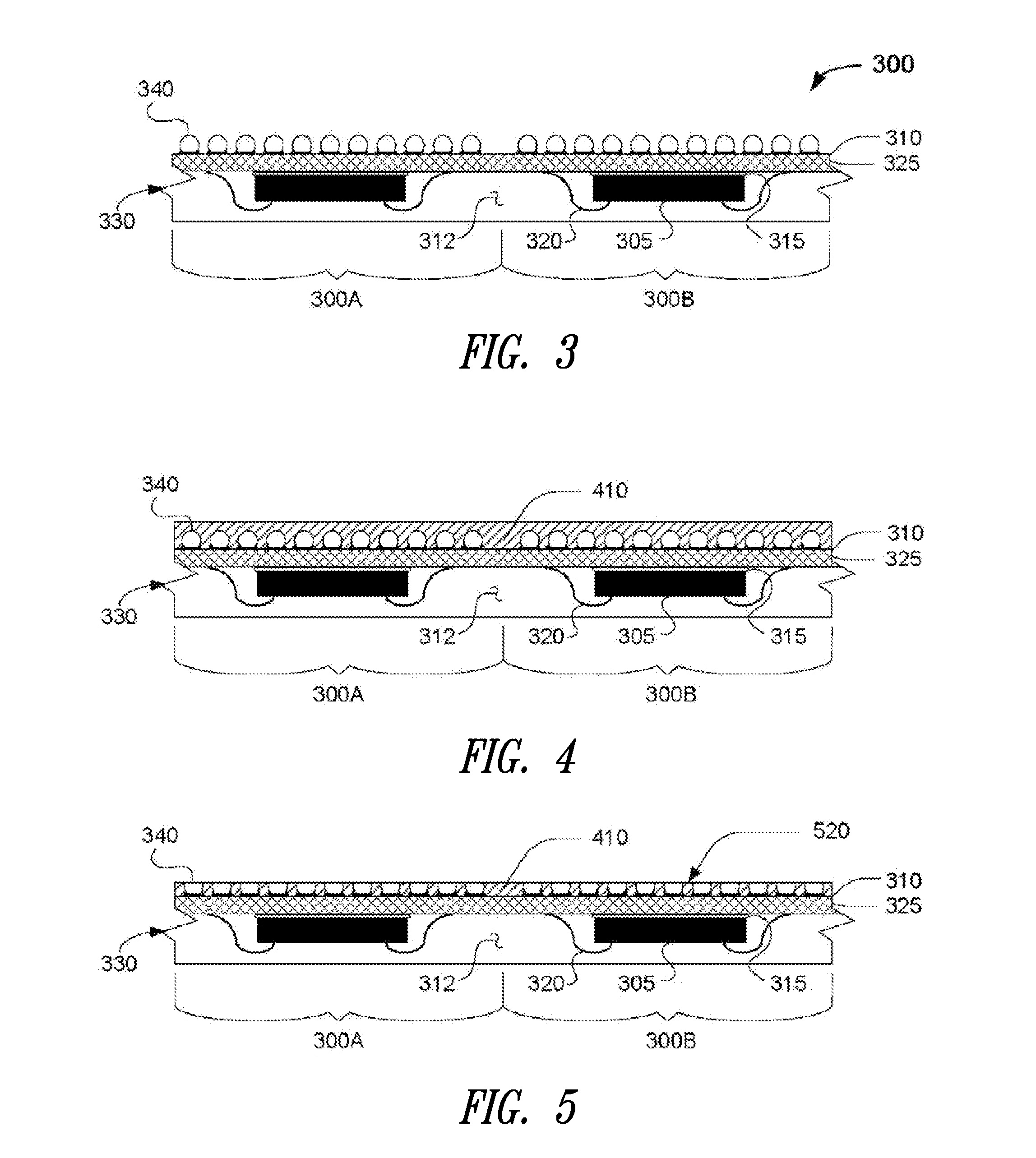
[0009]According to principles as explained herein, a pin grid array package is formed by first attaching solder balls to contact pads to create a standard ball grid array package. The solder balls are then encapsulated within a fixed material. A portion of the solder balls and a portion of the fixed

Problems solved by technology

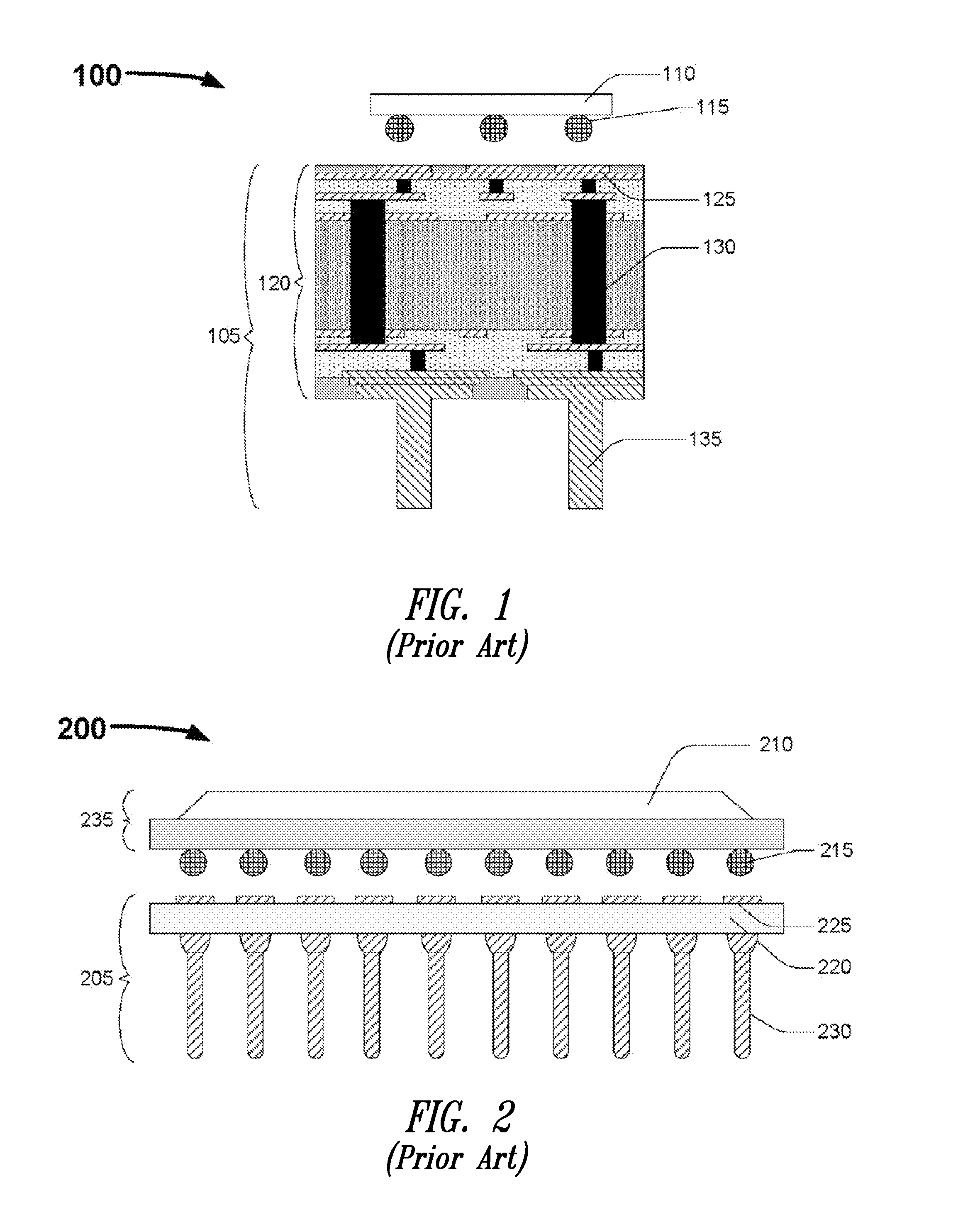
Currently costly different production lines are needed to manufacture BGA and PGA packages due to their inherently different physical architecture.
For every configuration of a ball grid array an entirely new design of an adaptor is needed, which requires additional time and tooling to prepare.
Additionally, the need to conserve space within small form factor devices may limit or otherwise restrict the ability to use an “oversize” external

Method used


Image

  • Ball grid array to pin grid array conversion
  • Ball grid array to pin grid array conversion
  • Ball grid array to pin grid array conversion

Examples


Embodiment Construction

[0024]In the following description, certain specific details are set forth in order to provide a thorough understanding of various disclosed embodiments. However, one skilled in the relevant art will recognize that embodiments may be practiced without one or more of these specific details, or with other methods, components, materials, etc.

[0025]Unless the context requires otherwise, throughout the specification and claims which follow, the word “comprise” and variations thereof, such as “comprises” and “comprising” are to be construed in an open, inclusive sense, that is, as “including, but not limited to.”

[0026]Reference throughout this specification to “one embodiment” or “an embodiment” means that a particular feature, structure, or characteristic described in connection with the embodiment is included in at least one embodiment. Thus, the appearances of the phrases “in one embodiment” or “in an embodiment” in various places throughout this specification are not necessarily all r...


PUM

PropertyMeasurementUnit
Temperatureaaaaaaaaaa
Melting pointaaaaaaaaaa

Abstract

Ball grid array to pin grid array conversion methods are provided. An example method can include coupling a plurality of solder balls to a respective plurality of pin grid array contact pads. Each of the plurality of solder balls is encapsulated in a fixed material. A portion of the plurality of solder balls and a portion of the fixed material is removed to provide a plurality of exposed solder balls. The exposed solder balls are softened and each of a plurality of pin members is inserted in a softened, exposed, solder ball. The plurality of pin members forms a pin grid array package.

Description

BACKGROUND[0001]1. Technical Field[0002]This disclosure generally relates to packaging of integrated circuits and particularly relates to conversion of ball grid array (BGA) packages to pin grid array (PGA) packages.[0003]2. Description of the Related Art[0004]The packaging of integrated circuits (ICs) frequently depends upon the expected method for board mounting the ICs. Two of the IC packaging methods in widespread use are ball grid array (BGA) packaging and pin grid array (PGA) packaging. The semiconductor die within a BGA packaged IC is electrically coupled to “pads” disposed on a surface of the BGA package. Small solder balls are bonded to each of the BGA contact pads. Coupling the BGA package to an underlying circuit board is accomplished by melting the solder to provide the electrical and physical coupling between the BGA package and the underlying circuit board. Since the BGA package is mounted directly on the circuit board, the board space and height of the mounted BGA pac...

Claims


Application Information

Patent Timeline
IPC IPC(8): H01L23/485B23K31/02B23K1/20
CPCB23K1/0016H01L24/97H01L2224/32225H01L2224/48227H01L2224/73265H01L2224/97H01L2924/15311H01L2924/15312H01L2924/00012H01L2224/83H01L2224/85H01L2924/00H01L24/73H01L2924/01322H01L2924/181
Inventor GOH, KIM-YONG
Owner STMICROELECTRONICS SRL
Why Eureka
Try Eureka