
Housing of electronic device and method for manufacturing same

a technology for electronic devices and housings, which is applied in the direction of electrical apparatus casings/cabinets/drawers, coupling device connections, details of portable computers, etc., can solve the problems of reducing the overall capability of being contained or containable in easy deformation of the sidewall of the housing when in use, and the effect of reducing the overall capacity of electronic devices

Inactive Publication Date: 2013-06-06
FU TAI HUA IND SHENZHEN +1
View PDF13 Cites 7 Cited by
  • Summary
  • Abstract
  • Description
  • Claims
  • Application Information

AI Technical Summary

Benefits of technology

The patent text describes a problem with the design of electronic devices, which are becoming thinner and thinner. This makes it difficult to contain the device in its housing and can cause the side of the housing to be easily deformed when in use. This can also lead to deformation of the connecting ports, which can affect the appearance and performance of the device. The technical effect is to provide a solution to these design issues to improve the design and make electronic devices more durable and reliable.

Problems solved by technology

Electronic devices are becoming thinner and thinner.
This reduces the overall capability of being contained or containable in the sidewall of the housing, and the sidewall of the housing is easily deformed when in use.
In addition, the connecting ports may be deformed, which affects the appearance of the electronic device and possibly its performance.

Method used


Image

  • Housing of electronic device and method for manufacturing same
  • Housing of electronic device and method for manufacturing same
  • Housing of electronic device and method for manufacturing same

Examples


Embodiment Construction

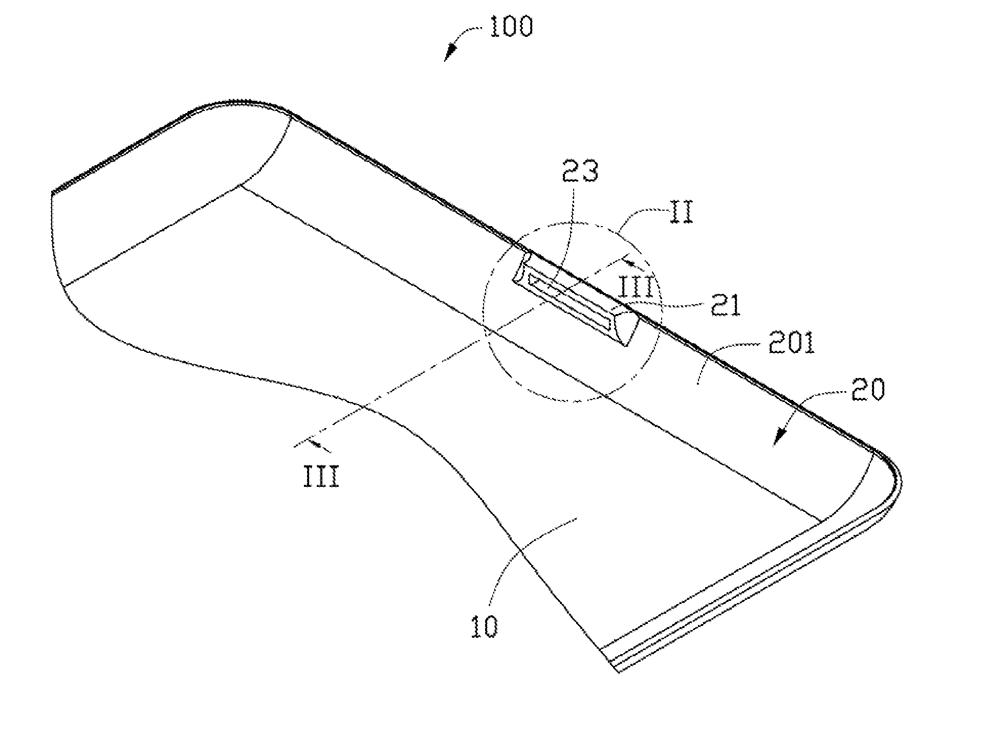
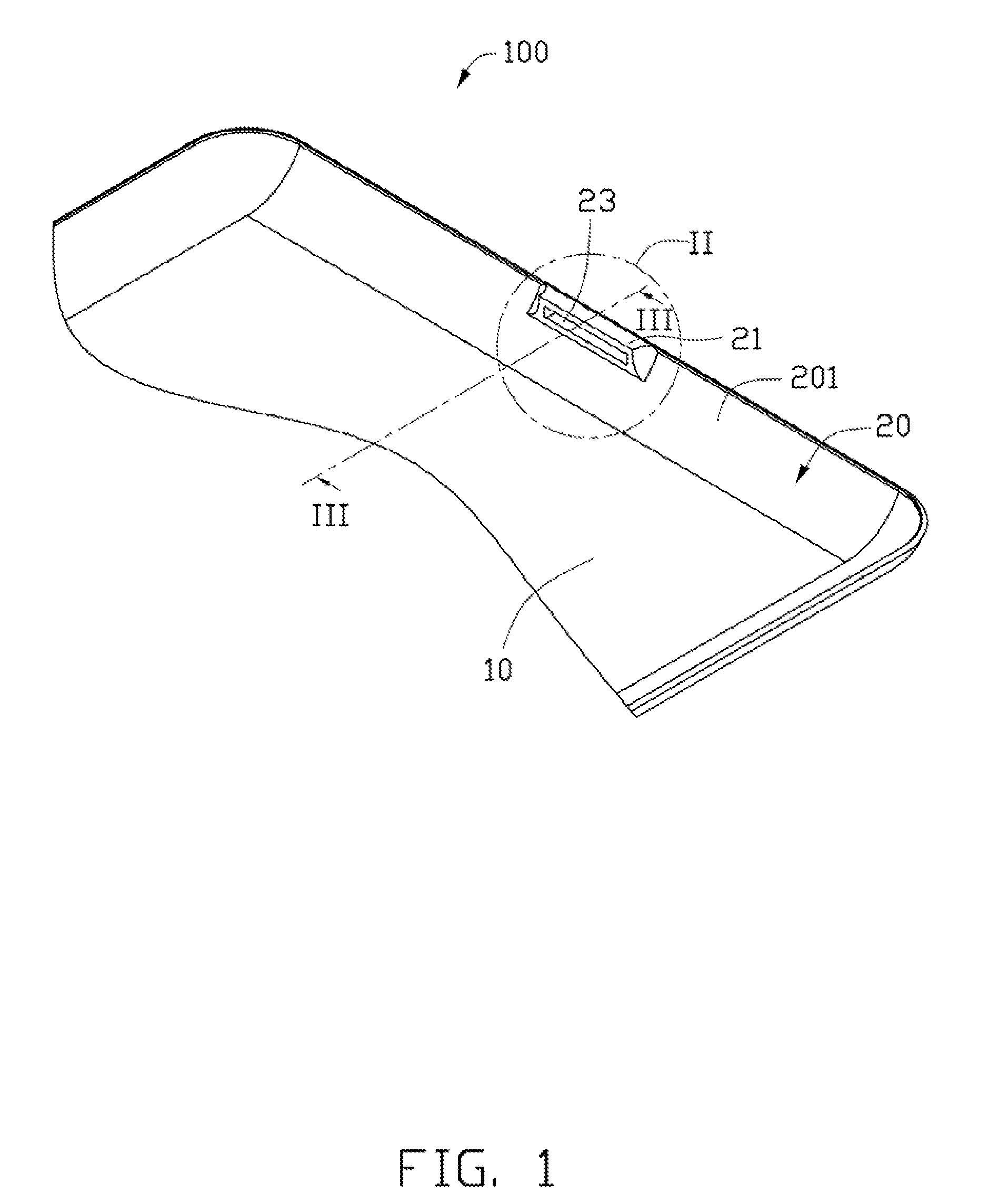
[0011]FIG. 1 shows an embodiment of a housing 100 (only shown in a partial isometric view) including a main body 10 and at least one sidewall 20. The sidewall 20 may curve upwards or downwards from an edge of the main body 10. In the illustrated embodiment, there are four sidewalls 20, and the four sidewalls 20 are connected end to end, respectively. The housing 100 is for an electronic device (not shown).

[0012]Referring to FIG. 3, the main body 10 is substantially a plate, and the sidewalls 20 are substantially a plurality of arcuate sheets. The housing 100 is made of one or more metallic materials. The main body 10 and the sidewalls 20 are pressed or milled from an integrated base material (not shown). In the illustrated embodiment, the housing 100 is made of aluminum.

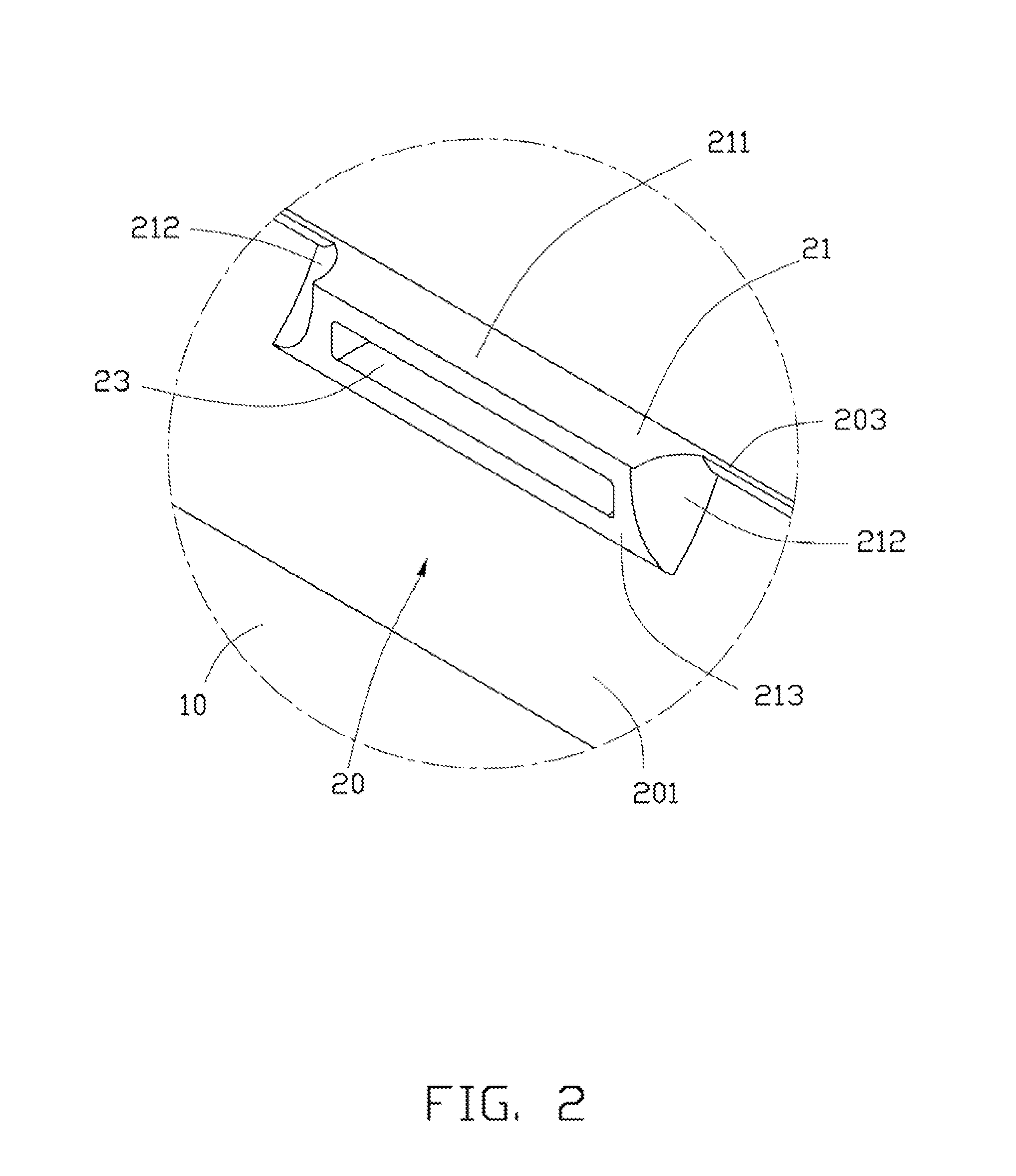
[0013]FIGS. 2 and 3 show one of the sidewalls 20 at an end of the main body 10 including an inner side surface 201, an outer side surface 202 opposite to the inner side surface 201 and a connecting edge 203 connectin...


PUM

PropertyMeasurementUnit
Thicknessaaaaaaaaaa
Angleaaaaaaaaaa
Metallic bondaaaaaaaaaa

Abstract

A housing of an electronic device includes a main body, at least one sidewall, and a strengthening portion. The sidewall bends outward from an edge of the main body. The sidewall includes an inner side surface adjacent to the main body and an outer side surface opposite to the inner side surface. The strengthening portion is located on the inner side surface of the at least one sidewall. The sidewall defines a connecting port at the outer side surface thereof, and the connecting port passes through the at least one sidewall and the strengthening portion. The present disclosure further provides a manufacturing method of the housing.

Description

BACKGROUND[0001]1. Technical Field[0002]The present disclosure relates to a housing, particularly to a housing of an electronic device and a method for manufacturing the housing.[0003]2. Description of Related Art[0004]A housing of an electronic device defines a plurality of connecting ports at a sidewall thereof, for connecting with another electronic device to exchange data. Electronic devices are becoming thinner and thinner. This reduces the overall capability of being contained or containable in the sidewall of the housing, and the sidewall of the housing is easily deformed when in use. In addition, the connecting ports may be deformed, which affects the appearance of the electronic device and possibly its performance.[0005]Therefore, there is room for improvement in the art.BRIEF DESCRIPTION OF THE DRAWINGS[0006]The components in the drawings are not necessarily drawn to scale, the emphasis instead being placed upon clearly illustrating the principles of the present disclosure...

Claims


Application Information

Patent Timeline
IPC IPC(8): H05K5/02B23P11/00
CPCH05K5/0247G06F1/1613G06F1/1616G06F1/1626Y10T29/49002H01R13/50H01R13/504H01R43/18H04M1/0274G06F1/181
Inventor DUAN, JU-PINGLUO, MING-FU
Owner FU TAI HUA IND SHENZHEN
Learn More