Semiconductor device packaging using encapsulated conductive balls for package-on-package back side coupling

a technology of conductive balls and semiconductor devices, applied in the direction of semiconductor devices, semiconductor/solid-state device details, electrical apparatus, etc., can solve the problems of high cost of materials, process and additional tooling to generate through vias and interconnections

Inactive Publication Date: 2013-06-20
FREESCALE SEMICON INC
View PDF5 Cites 32 Cited by
  • Summary
  • Abstract
  • Description
  • Claims
  • Application Information

AI Technical Summary

Problems solved by technology

This process of post-encapsulation via and interconnect formation introduces complexities to the manufacturing process that have a variety of manufacturing an

Method used


Image

  • Semiconductor device packaging using encapsulated conductive balls for package-on-package back side coupling
  • Semiconductor device packaging using encapsulated conductive balls for package-on-package back side coupling
  • Semiconductor device packaging using encapsulated conductive balls for package-on-package back side coupling

Examples


Embodiment Construction

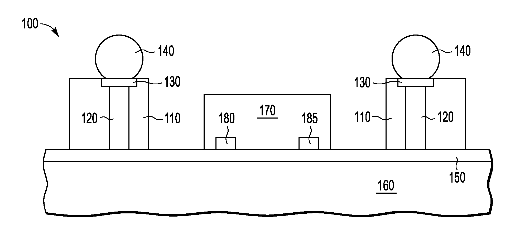
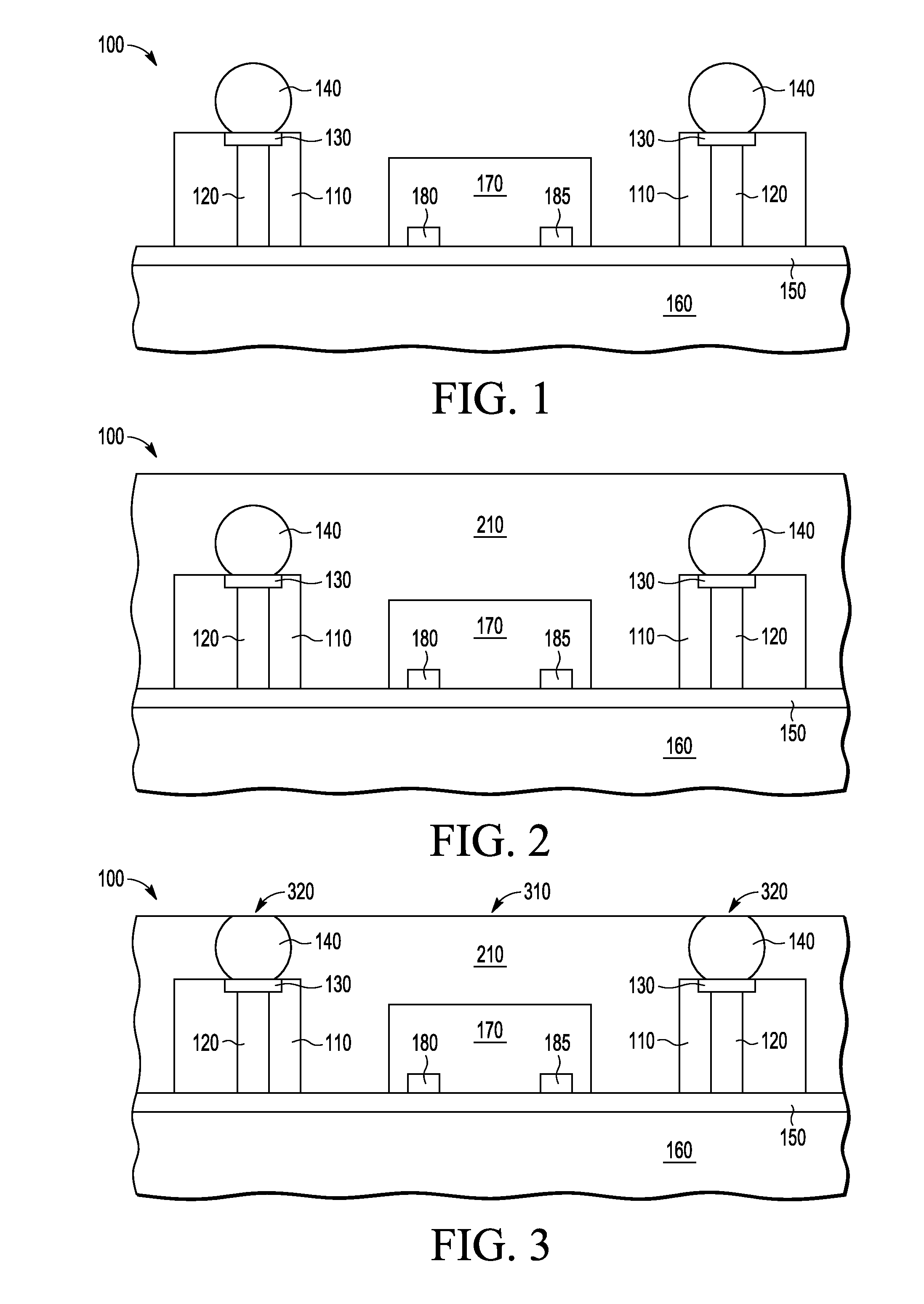
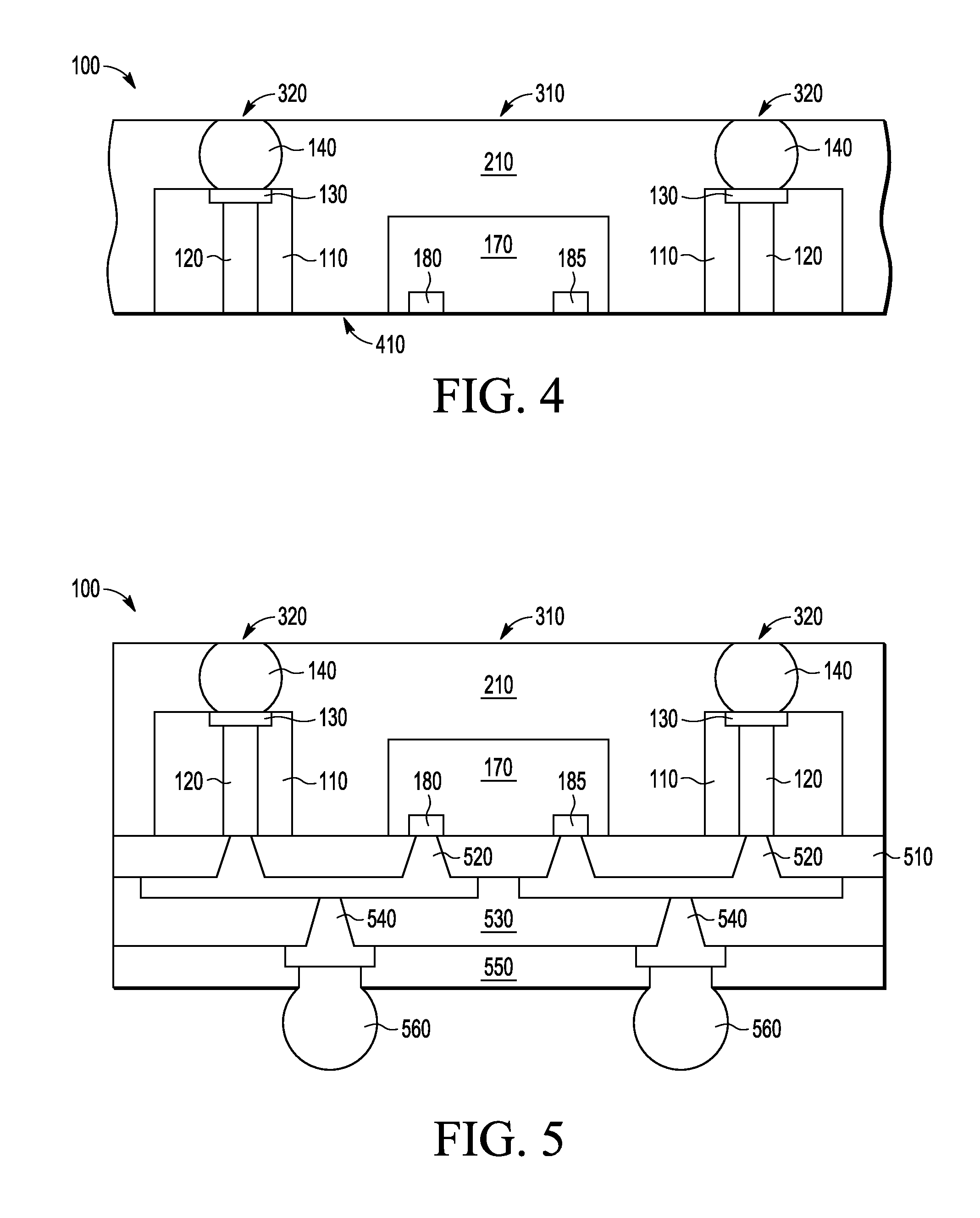
[0017]A semiconductor device package having an embedded three-dimensional interconnect structure and a process for making such a package is provided. One or more ball conductors or similar structures (e.g., gold studs) are attached to a major surface of a substrate that provides at least an electrical conduit (e.g., conductive pillars) from the ball conductor to an opposite major surface of the substrate. In addition, the substrate can provide a two-dimensional interconnect between ball conductors. The combination of ball conductors and substrate is subsequently embedded in an encapsulated semiconductor device package. The ends of the signal conduits are exposed on one major surface of the device package, while the opposite major surface of the device package is back grinded (or the equivalent) to expose a portion of the ball conductors. The conductive pathway of ball conductors and signal conduits are then used as through vias, providing signal-bearing pathways between the bottom a...


PUM


Abstract

A semiconductor device package having an embedded three-dimensional interconnect structure and a process for making such a package is provided. One or more ball conductors are attached to a major surface of a substrate that provides at least an electrical conduit from the ball conductor to an opposite major surface of the substrate. The substrate can also provide an interconnect between solder balls. The combination of solder balls and substrate is encapsulated in the semiconductor device package. The ends of the signal conduits are exposed on one major surface of the device package, while a portion of the ball conductors is exposed on the opposite major surface of the device package. The ball conductors and signal conduits provide signal-bearing pathways between the major surfaces of the package. Contacts created by the back grinded ball conductors are used to form a package-on-package structure by coupling with contacts from another package.

Description

BACKGROUND[0001]1. Field[0002]This disclosure relates generally to semiconductor device packaging, and more specifically, to providing through-package vias and back side coupling in an encapsulated device package by using pre-formed signal conduits and conductive balls.[0003]2. Related Art[0004]Semiconductor and other types of electronic devices are often encapsulated wholly or partly in resin to provide environmental protection and facilitate external connection to the devices. Subsequent to encapsulation, interconnect structures can be built up on one or both sides of the encapsulated devices to allow for package-on-package arrangements. For packages having electrical contacts on both top and bottom surfaces (e.g., a double-sided buildup), through-vias are often made to provide contacts between bottom side and top side interconnect structures. Traditionally, through package vias are made after encapsulation using a drilling and filling / metallization process that includes steps for...

Claims


Application Information

Patent Timeline
IPC IPC(8): H01L23/498H01L21/50
CPCH01L23/49816H01L23/4985H01L23/5389H01L25/105H01L21/568H01L2924/15311H01L24/19H01L24/20H01L2224/12105H01L2225/1035H01L2225/1058H01L23/552H01L2924/181H01L2924/00
Inventor WRIGHT, JASON R.GONG, ZHIWEIHAYES, SCOTT M.MITCHELL, DOUGLAS G.
Owner FREESCALE SEMICON INC
Why Eureka
Try Eureka