

Driver circuit
- Summary
- Abstract
- Description
- Claims
- Application Information
AI Technical Summary
Benefits of technology
Problems solved by technology
Method used
Image

Examples
first embodiment
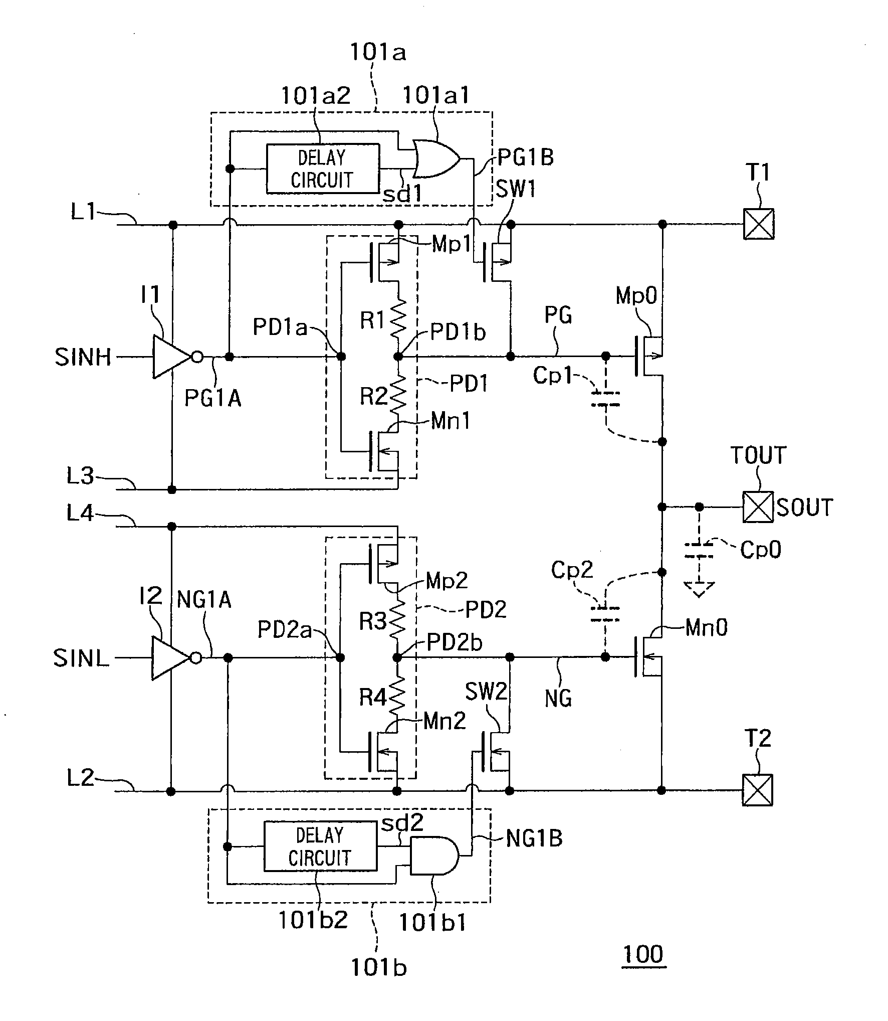
[0016]FIG. 1 is a circuit diagram showing an example of a configuration of a driver circuit 100 according to a first embodiment.
[0017]As shown in FIG. 1, the driver circuit 100 includes a first terminal “T1”, a second terminal “T2”, an output terminal “TOUT”, first to fourth potential lines “L1” to “L4”, an output pMOS transistor “Mp0”, an output nMOS transistor “Mn0”, an auxiliary pMOS transistor “SW1”, an auxiliary nMOS transistor “SW2”, a first pre-driver circuit “PD1”, a second pre-driver circuit “PD2”, a first controlling circuit 101a, a second controlling circuit 101b, a first inverter “I1”, and a second inverter “I2”.
[0018]A first potential (power supply potential, for example) is applied to the first terminal “T1”.
[0019]A second potential (ground potential, for example) lower than the first potential is applied to the second terminal “T2”.
[0020]The first potential line “L1” is connected to the first terminal “T1”, for example. In this case, the potential of the first potenti...
second embodiment
[0070]In the first embodiment, there has been described an example of the configuration that generates controlling signals that control the auxiliary MOS transistors from signals after generation of the dead time.
[0071]In a second embodiment, there will be described an example of the configuration that generates controlling signals that control the auxiliary MOS transistors at the same time as generating signals including a dead time.
[0072]FIG. 3 is a circuit diagram showing an example of a configuration of a driver circuit 200 according to the second embodiment. In FIG. 3, the same reference symbols as those in FIG. 1 denote the same components as those in the first embodiment.
[0073]As shown in FIG. 3, the driver circuit 200 includes the first terminal “T1”, the second terminal “T2”, the output terminal “TOUT”, the first to fourth potential lines “L1” to “L4”, the output pMOS transistor “Mp0”, the output nMOS transistor “Mn0”, the auxiliary pMOS transistor “SW1”, the auxiliary nMOS...
third embodiment
[0102]In a third embodiment, there will be described another example of the configuration that generates controlling signals that control the auxiliary MOS transistors at the same time as generating signals including a dead time.
[0103]FIG. 5 is a circuit diagram showing an example of a configuration of a driver circuit 300 according to the third embodiment. In FIG. 5, the same reference symbols as those in FIG. 3 denote the same components as those in the second embodiment.
[0104]As shown in FIG. 5, the driver circuit 300 includes the first terminal “T1”, the second terminal “T2”, the output terminal “TOUT”, the first to fourth potential lines “L1” to “L4”, the output pMOS transistor “Mp0”, the output nMOS transistor “Mn0”, the auxiliary pMOS transistor “SW1”, the auxiliary nMOS transistor “SW2”, the first pre-driver circuit “PD1”, the second pre-driver circuit “PD2”, a first controlling circuit 301a, and a second controlling circuit 301b.
[0105]The first controlling circuit 301a dif...
PUM
 Abstract
Description
Claims
Application Information