Method for manufacturing nitride semiconductor device and the same manufactured thereof

a technology of nitride semiconductor and semiconductor device, which is applied in the direction of semiconductor devices, electrical devices, transistors, etc., can solve the problems of reducing the maximum drain current at an on-state, affecting the performance of the device, and requiring several nm etching depth control, etc., so as to improve the performance reduce the leakage current on the surface, and improve the effect of the high-power elemen

Inactive Publication Date: 2013-09-26
LG ELECTRONICS INC
View PDF5 Cites 3 Cited by
  • Summary
  • Abstract
  • Description
  • Claims
  • Application Information

AI Technical Summary

Benefits of technology

[0029]Exemplary aspects of the present disclosure have an advantageous effect in that devices are manufactured using a growth without recourse to etching process to enable a several-nanometer control.
[0030]Another advantageous effect is that a leakage current on a surface can be greatly reduced due t...

Problems solved by technology

Although an HFET (Heterojunction Field Effect Transistor) structure based on nitride semiconductors has high electron mobility for application in communication devices of harmonic characteristics, the HFET poses a problem of generating a so-called “normally-on” phenomenon due to its structural characteristics.
This method however poses a problem of resulting in decrease a maximum drain current at an on-state due to reduction in the 2DEG concentration serving as a channel.
However, the disadvantage is that the HFET structure essentially requires a several nm etching depth control because an increased cha...

Method used


Image

  • Method for manufacturing nitride semiconductor device and the same manufactured thereof
  • Method for manufacturing nitride semiconductor device and the same manufactured thereof
  • Method for manufacturing nitride semiconductor device and the same manufactured thereof

Examples


Embodiment Construction

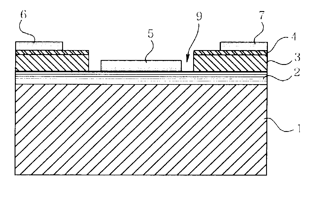
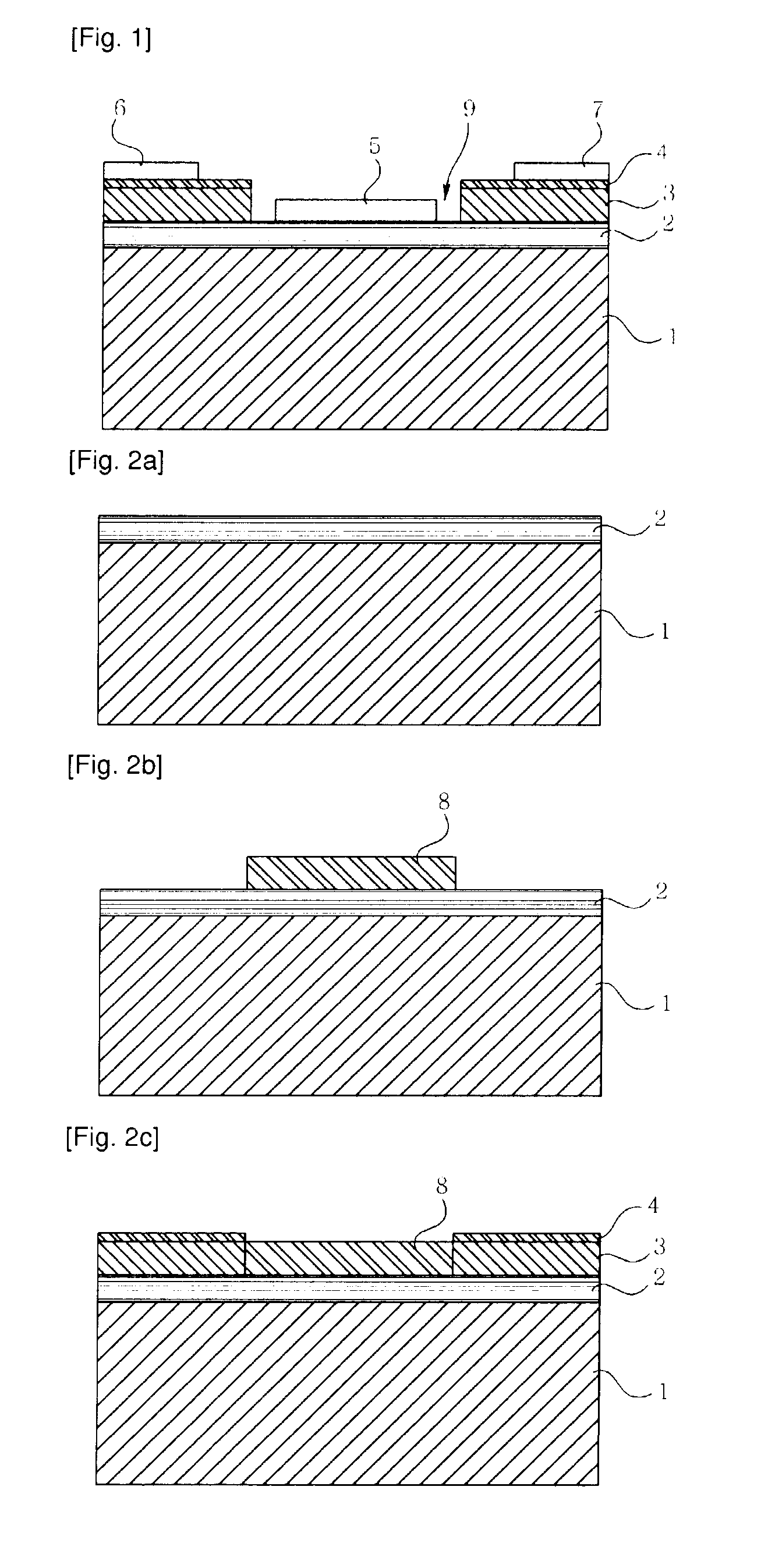
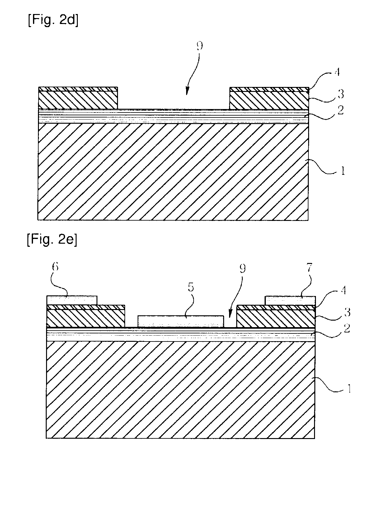
[0035]Various exemplary embodiments will be described more fully hereinafter with reference to the accompanying drawings, in which some exemplary embodiments are shown.

[0036]The present inventive concept may, however, be embodied in many different forms and should not be construed as limited to the example embodiments set forth herein. Rather, the described aspect is intended to embrace all such alterations, modifications, and variations that fall within the scope and novel idea of the present disclosure.

[0037]It will be understood that, although the terms first, second etc. may be used herein to describe various elements, components, regions, layers and / or sections, these elements, components, regions, layers and / or sections should not be limited by these terms.

[0038]These terms are only used to distinguish one element, component, region, layer or section from another region, layer or section. Thus, a first element, component, region, layer or section discussed below could be t...


PUM


Abstract

Disclosed is a nitride semiconductor device and a method for manufacturing the same and the method for manufacturing the nitride semiconductor device comprising: growing a buffer layer including a first semiconductor on a substrate; growing a first barrier layer including a second semiconductor different from the first semiconductor; forming an oxide film layer on a portion where a recess is to be formed; growing a second barrier layer including the second semiconductor; forming a recess by removing the oxide film layer; and forming a gate electrode on the recess.

Description

BACKGROUND OF THE DISCLOSUREField of Endeavor[0001]The teachings in accordance with exemplary and non-limiting embodiments of this disclosure relate generally to a semiconductor device, and more particularly to a HFET (Heterojunction Field-Effect Transistor) and a method for manufacturing the same.Background[0002]In general, nitride-based semiconductors are wide bandgap compound semiconductors capable of emitting light ranging from visible light to ultraviolet light.[0003]The nitride-based semiconductors applied to emit light such as blue purple light emitting diodes or laser diodes and blue light emitting diodes are already developed for wide use in light pick-up devices, traffic lights, public displays, liquid crystal backlight illuminations and mobile terminals.[0004]Gallium nitride (GaN), one of representative materials for semiconductors, is being widely studied recently as a material for semiconductor devices due to its advantageous characteristics such as higher breakdown vol...

Claims


Application Information

Patent Timeline
IPC IPC(8): H01L29/80H01L29/66
CPCH01L29/2003H01L29/66462H01L29/802H01L29/66431H01L29/7787H01L29/73H01L29/737H01L29/778
Inventor JANG, TAEHOONEUM, YOUNGSHIN
Owner LG ELECTRONICS INC
Why Eureka
Try Eureka