Method for printed circuit board trace characterization

a technology of printed circuit boards and trace characterization, which is applied in the direction of electronic circuit testing, measurement devices, instruments, etc., can solve the problems of degrading communication capability, reducing communication efficiency, and traditional methods that have not been successful, and achieves the effect of convenient utilization of the same test coupon structure, fast and easy-to-use methods

Active Publication Date: 2013-10-10
TELEDYNE LECROY
View PDF5 Cites 11 Cited by
  • Summary
  • Abstract
  • Description
  • Claims
  • Application Information

AI Technical Summary

Benefits of technology

[0013]It is an object of this invention to preferably provide a fast, easy and economical method for providing PCB trace characteristics measurements. It is further an object of this invention to preferably facilitate the utilization of the same t...

Problems solved by technology

When elements in the path of a high-speed signal have different characteristic impedances, reflections occur which may degrade communications.
When a trace is excessively lossy signals may be attenuated at high frequencies and again, the communications capability is degraded.
These traditional methods have been less successful as of late, especially when the traces are to be used with high speed data transfers.
There are several problems with this situation.
First, for many PCB manufacturers, high-frequency electrical characteristics are a domain of engineering that is foreign to them.
Next, the measurement of high-frequency characteristics are difficult and often time consuming.
Finally, the equipment needed to perform these measurements is very expensive.
VNA instruments...

Method used


Image

  • Method for printed circuit board trace characterization
  • Method for printed circuit board trace characterization
  • Method for printed circuit board trace characterization

Examples


Embodiment Construction

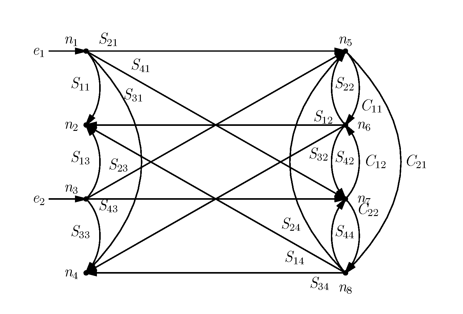
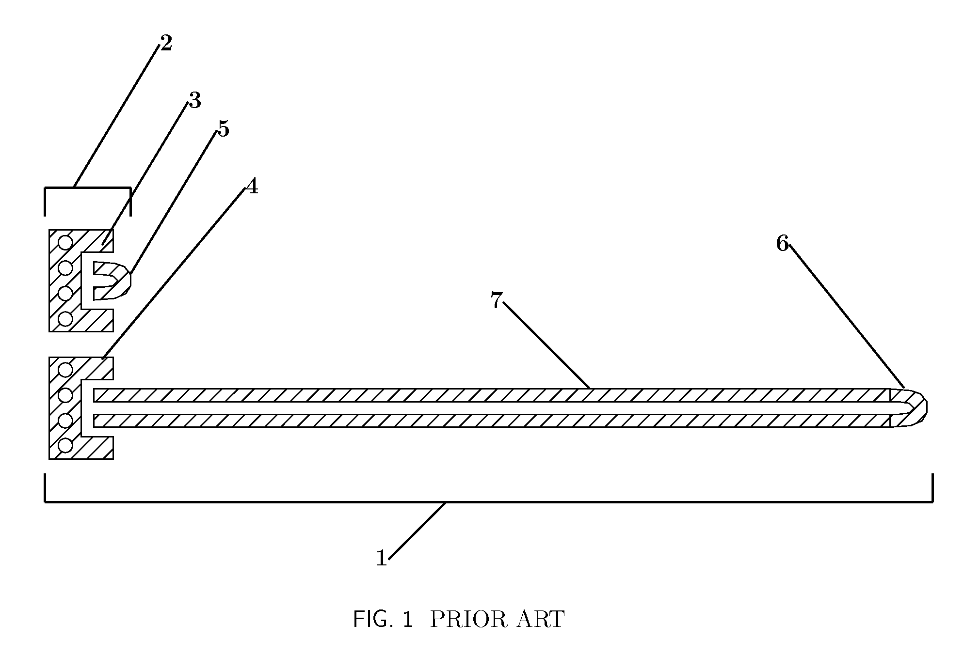
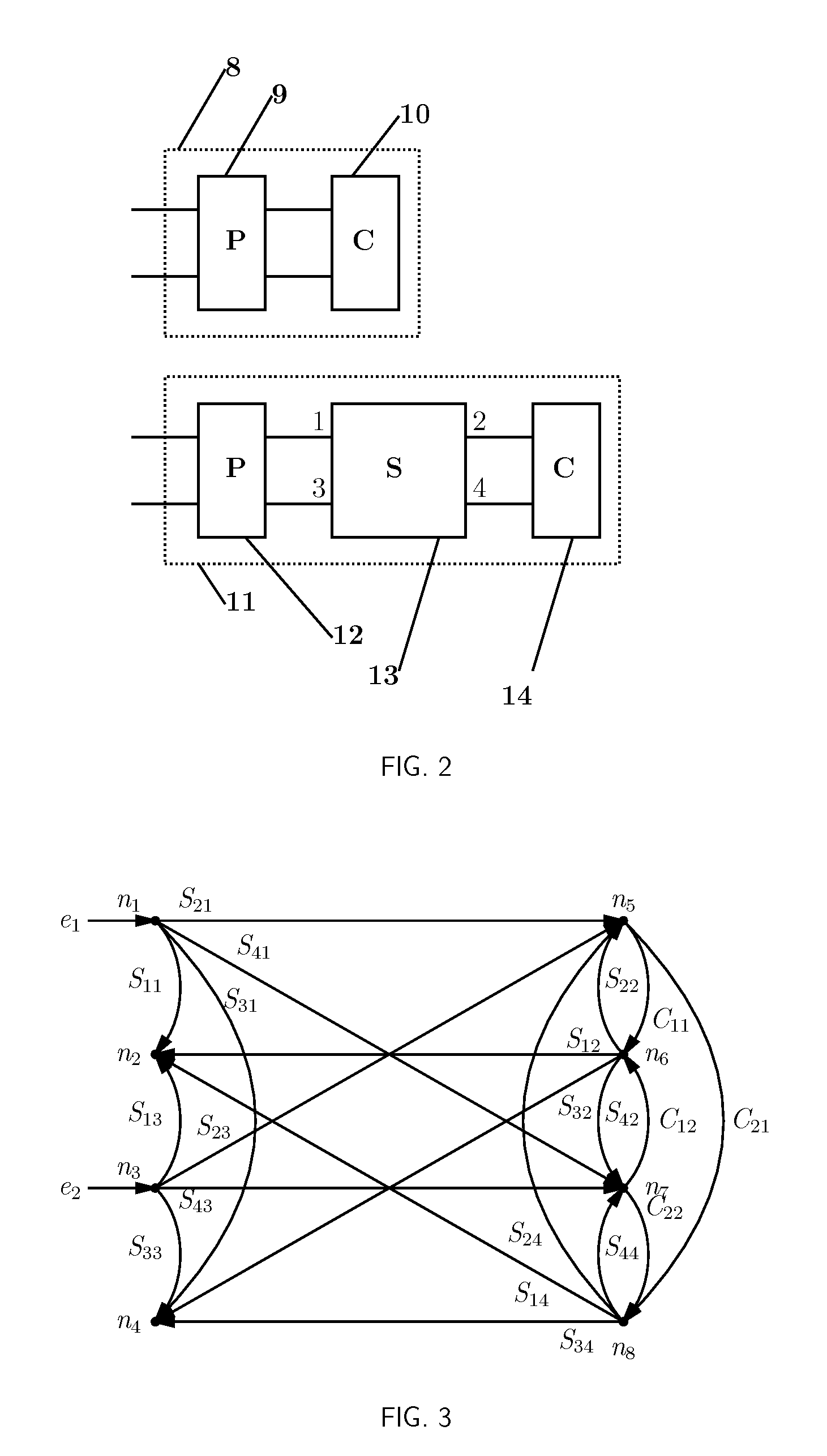
[0034]FIG. 1 shows elements of an exemplary test-coupon that may be employed for a PCB trace characterization measurement. It shows a trace characterization structure [1] and a termination characterization structure [2]. Both structures [1],[2] are intended to be substantially similar in that each contains a probing structure [3], [4] and a termination structure [5], [6] except that the trace characterization structure [1] contains a differential trace element [7] which is the DUT and is the element to be characterized.

[0035]The intent of the structures in FIG. 1 is that measurements are obtained for the trace characterization structure [1] and for the termination characterization structure [2] by probing and measuring each one. Based on these measurements, one or more characteristics of the DUT may be obtained.

[0036]Assuming that the termination structures [5], [6] are substantially similar and that a good measurement can be made of the termination structure [5] by measuring at the...


PUM


Abstract

A method is provided which measures PCB trace characteristics from measurements of a PCB trace structure.

Description

FIELD OF THE INVENTION[0001]The present invention relates in general to the measurement of electrical characteristics of printed circuit boards, and more particularly to the testing of one or more characteristics required for traces that propagate high-speed signals as en-countered in serial data communications.BACKGROUND OF THE INVENTION[0002]The printed circuit board (PCB) is an element in many electronic products that contain electronic components. The PCB holds components and connects these components electrically through metal traces. In some applications, especially high speed serial data communications, high quality traces are required. Thus the characteristics of these metal traces must be measured and tested to ensure high quality.[0003]Until relatively recently, the determination PCB and PCB trace quality meant the determination of the ability to handle current or voltage and or electrical resistance. As of late, however, many high-speed PCB traces are tested for character...

Claims


Application Information

Patent Timeline
IPC IPC(8): G01R31/28
CPCG01R31/2818
Inventor PUPALAIKIS, PETER J.DOSHI, KAVIYESH
Owner TELEDYNE LECROY
Why Eureka
Try Eureka