FinFET NON-VOLATILE MEMORY AND METHOD OF FABRICATION

a non-volatile memory and memory technology, applied in the direction of basic electric elements, semiconductor devices, electrical equipment, etc., can solve the problem of low drive curren

Inactive Publication Date: 2013-10-17
GLOBALFOUNDRIES INC
View PDF3 Cites 20 Cited by
  • Summary
  • Abstract
  • Description
  • Claims
  • Application Information

AI Technical Summary

Problems solved by technology

The main drawback of such a structure is its low drive current due to the thick gate oxide.

Method used


Image

  • FinFET NON-VOLATILE MEMORY AND METHOD OF FABRICATION
  • FinFET NON-VOLATILE MEMORY AND METHOD OF FABRICATION
  • FinFET NON-VOLATILE MEMORY AND METHOD OF FABRICATION

Examples


Embodiment Construction

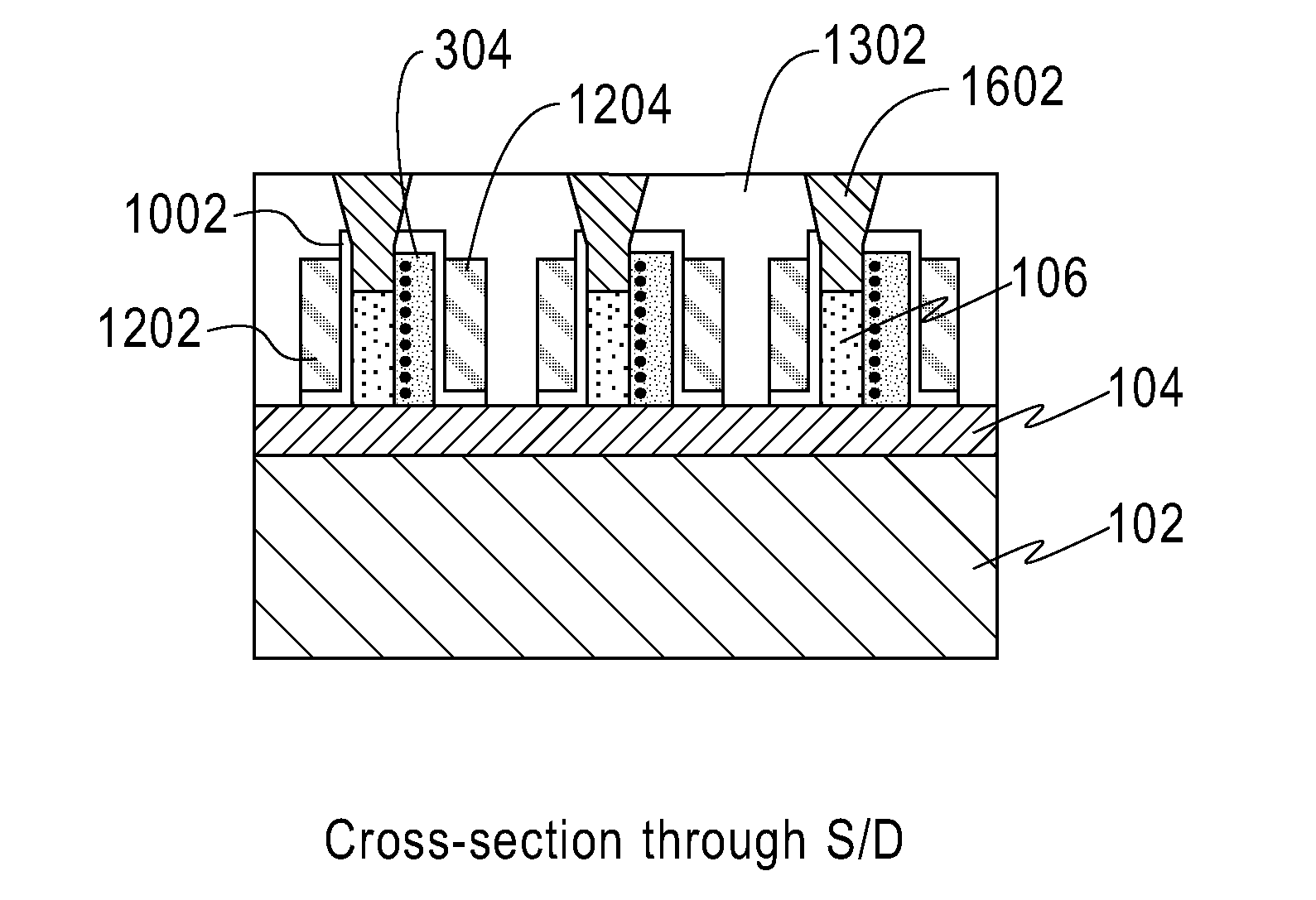
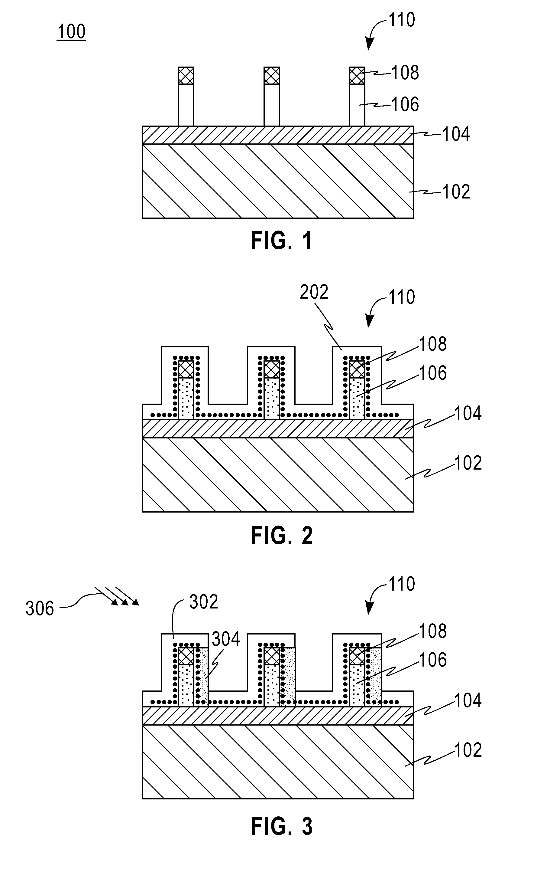
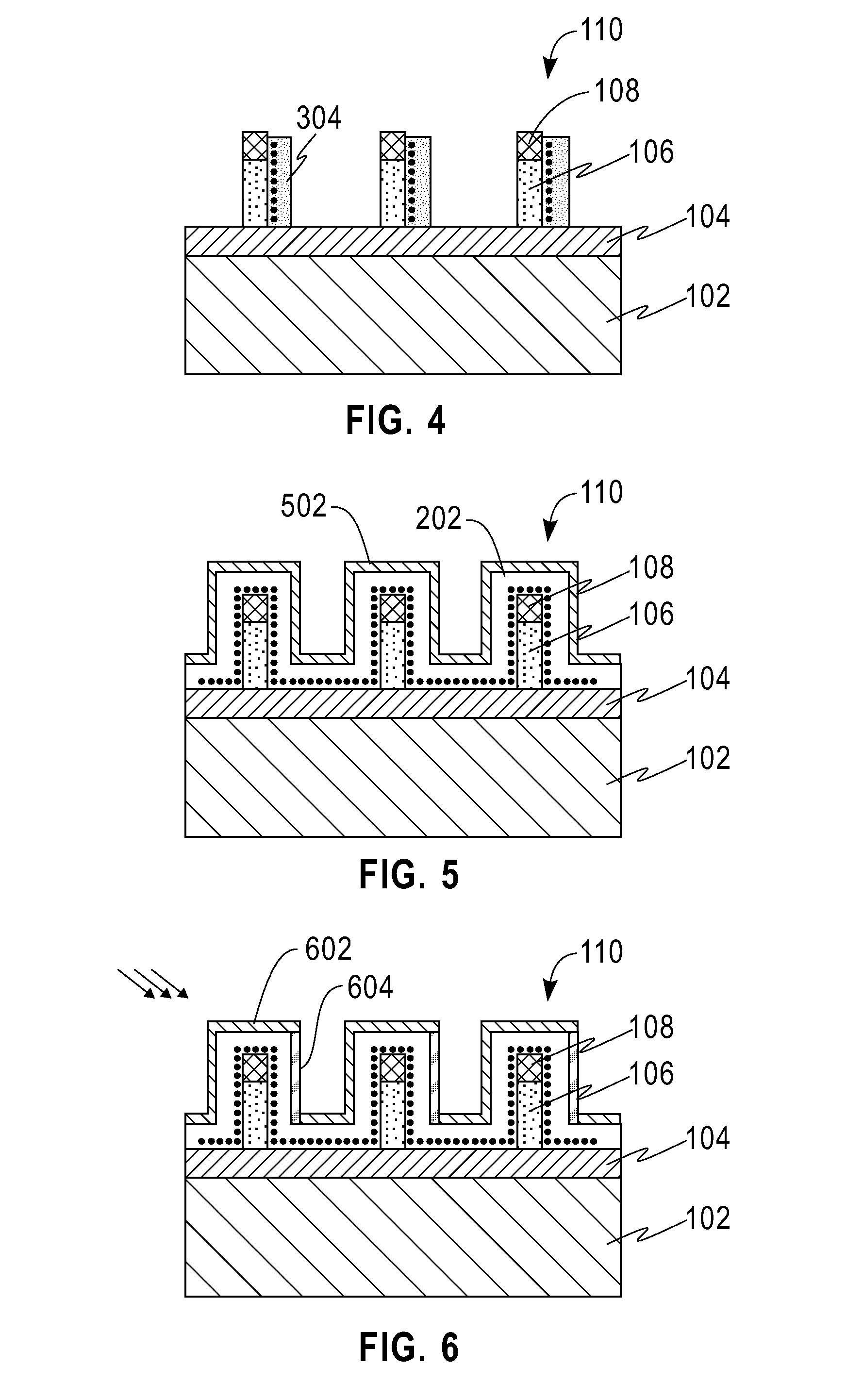
[0027]With reference now to FIG. 1, a cross-sectional view of one embodiment of a FinFET non-volatile memory device in an early stage of production is shown. Device 100 includes a semiconductor layer 102 and an insulating layer 104 formed over the semiconductor layer 102. Fin structure 110 is formed over insulating layer 104. In another embodiment, fin structure 110 can be formed over a strained silicon-on-insulator (sSOI) substrate. In other embodiments, the fin structure 110 can be formed over a bulk semiconductor substrate, including silicon, germanium, and the like. The embodiments described herein are not restricted to any specific semiconductor substrate configuration unless explicitly stated in an embodiment or the claims. Fin structure 110 includes a semiconductor portion 106 and a hard mask portion 108. In an embodiment, the semiconductor portion is silicon. In an embodiment, the hard mask 108 is a dielectric material, such as silicon dioxide, silicon nitride, silicon oxyni...


PUM


Abstract

A method of manufacturing a FinFET non-volatile memory device and a FinFET non-volatile memory device structure. A substrate is provided and a layer of semiconductor material is deposited over the substrate. A hard mask is deposited over the semiconductor material and the structure is patterned to form fins. A charge storage layer is deposited over the structure, including the fins and the portions of it are damaged using an angled ion implantation process. The damaged portions are removed and gate structures are formed on either side of the fin, with only one side having a charge storage layer.

Description

BACKGROUND OF THE INVENTION[0001]1. Field of the Invention[0002]The present invention generally relates to a non-volatile memory device, and more specifically to a FinFET non-volatile memory device.[0003]2. Description of Related Art[0004]Embedded non-volatile memory cells can add significant functionality to integrated circuits. Flash cells based on FinFET, trigate, or nanowire transistors are especially of interest because of excellent short channel control offered by these device structures which provide better device scalability compared to bulk devices. Different cells based on these devices have been proposed in recent years with an ONO, high-k, or nano-crystal charge storage element that surrounds the entire channel. The main drawback of such a structure is its low drive current due to the thick gate oxide. In planar SOI devices, it is possible to decouple the write and read operation by placing the storage element inside the BOX. The front gate oxide can then be scaled as ag...

Claims


Application Information

Patent Timeline
Patent Type & Authority Applications(United States)
IPC IPC(8): H01L27/12H01L21/336
CPCH01L21/845H01L29/66795H01L29/785H01L29/42328H01L29/42332H01L29/42344H01L29/66825H01L29/66833H01L29/7881H01L29/792H01L29/40114H01L29/40117H01L21/823431H10B41/35H10B43/30H10B43/35H10B41/30
Inventor CHENG, KANGGUODORIS, BRUCE B.KHAKIFIROOZ, ALIKULKARNI, PRANITA
Owner GLOBALFOUNDRIES INC
Why Eureka
Try Eureka