
Display Panel and Display Device Having the Same

Inactive Publication Date: 2013-10-24
SAMSUNG DISPLAY CO LTD
View PDF6 Cites 16 Cited by
  • Summary
  • Abstract
  • Description
  • Claims
  • Application Information

AI Technical Summary

Benefits of technology

This patent describes an apparatus for improving the display of a display device by reducing the delay in the transmission of data signals through the display device. The apparatus includes a delay compensating line and a delay compensating transistor that synchronizes the timing of the data signals to reduce the delay in the display device. By driving the delay compensating transistor every frame, the apparatus prevents degradation and ensures a consistent quality display. The technical effect of this invention is improved display efficiency and consistent quality.

Problems solved by technology

However, the number of gate drive circuits of a gate driving part increases when using the dual gate driving part, such that manufacturing costs increase and the size of a bezel expands.
However, when the gate driving signal is applied to merely one terminal of the gate line, the gate driving signal may not have enough of a charge transfer period with respect to the load of the gate line and an RC delay may result.

Method used


Image

  • Display Panel and Display Device Having the Same
  • Display Panel and Display Device Having the Same
  • Display Panel and Display Device Having the Same

Examples


Embodiment Construction

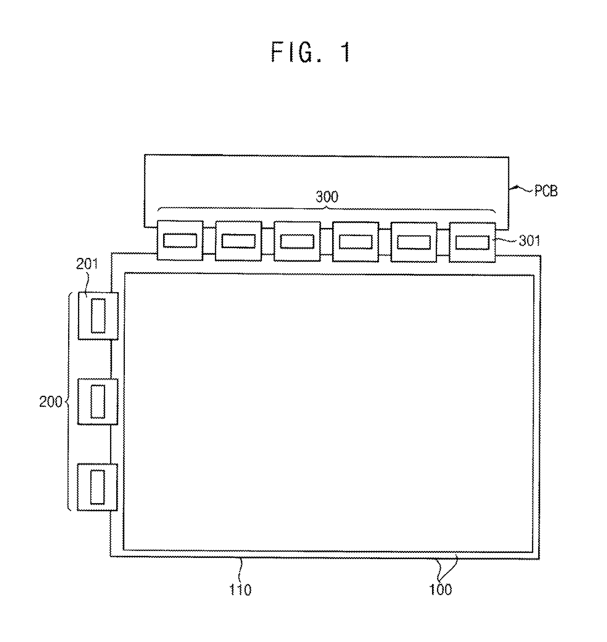
[0046]Referring to FIGS. 1 to 3, the display device includes a display panel 100, a gate driving part 200 disposed on an edge of the display panel 100 and a data driving part 300 disposed on another edge of the display panel 100. The display device may further include a printed circuit board (PCB) connected to the data driving part 300.

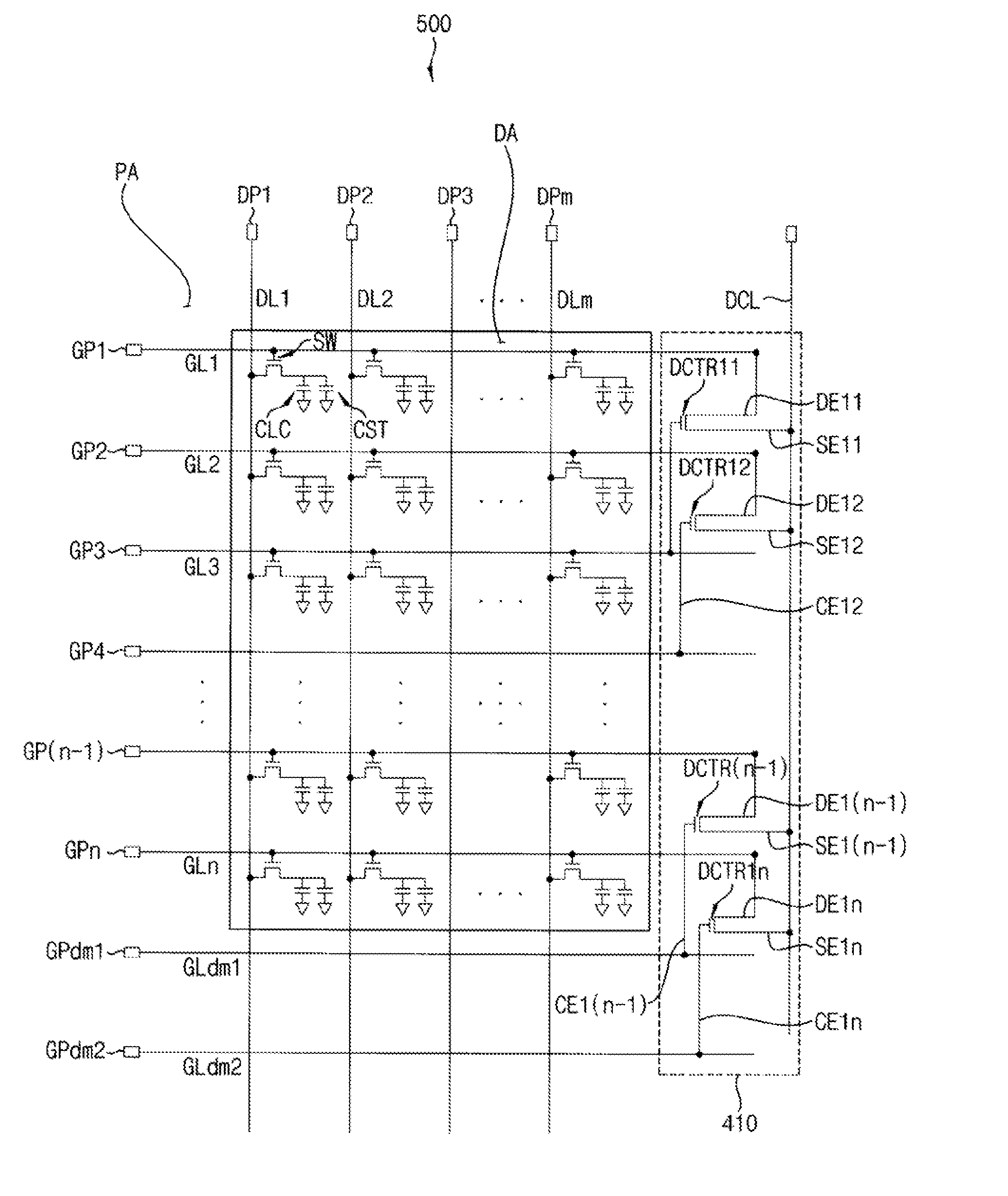
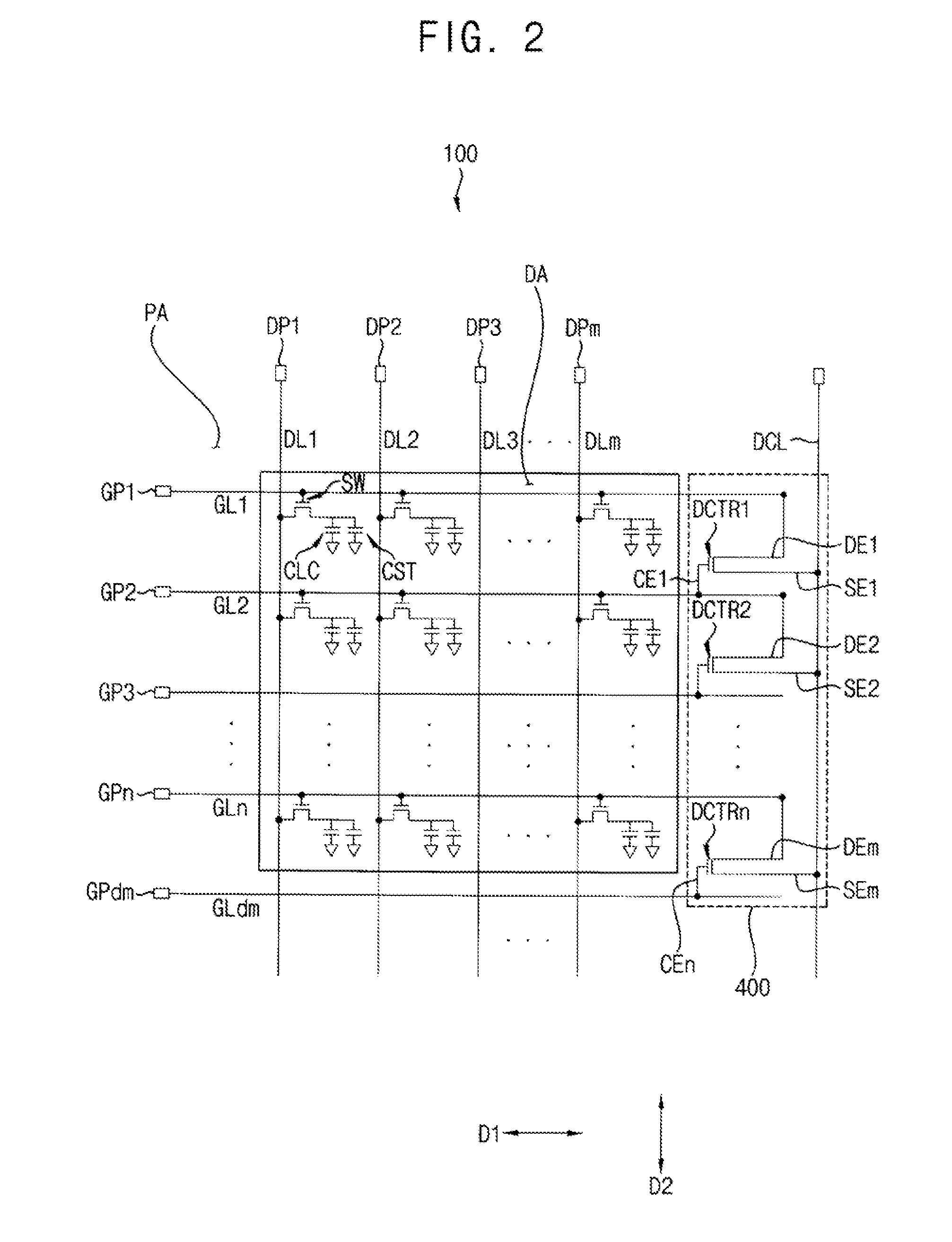
[0047]The display panel 100 includes a display substrate which includes a base substrate 110, a plurality of gate lines GL1, . . . , GL(n−1), GLn disposed on the base substrate 110, a plurality of gate pads GP1, . . . , GP(n−1), GPn, a dummy gate line GLdm, a dummy gate pad GPdm, a plurality of data lines DL1, . . . , DL(m−1), DLm, a plurality of data pads DP1, . . . , DP(m−1), DPm, switching elements and a delay compensating circuit 400, liquid crystal capacitors CLC and storage capacitors CST.

[0048]The gate lines GL1, . . . , GL(n−1), GLn and the dummy gate line GLdm extend in a first direction D1. The dummy gate line GLdm is disposed adjacent to ga...


PUM


Abstract

A display panel includes a base substrate, a first gate line, a second gate line, first and second gate pads, a data line, a delay compensating line and a first delay compensating transistor. The first gate line extends in a first direction on the base substrate. The second gate line is substantially parallel to the first gate line. The first and second gate pads extend from first terminals of respective first and second gate lines. The data line extends in a second direction which is different from the first direction. The delay compensating line is substantially parallel to the data line. The first delay compensating transistor is electrically connected to the first and second gate lines and to the delay compensating line.

Description

CROSS-REFERENCE TO RELATED APPLICATION[0001]This application claims under 35 U.S.C. §119 priority to and the benefit of Korean Patent Application No. 10−2012−0041328, filed on Apr. 20, 2012 in the Korean Intellectual Property Office (KIPO), the entire contents of which are incorporated by reference herein.BACKGROUND[0002]1. Technical Field[0003]The present disclosure relates to a display panel and a display device having the display panel, and, more particularly, to a display panel that has a delay compensating circuit.[0004]2. Discussion of the Related Art[0005]A display device typically includes a display panel, a gate driving part that applies a gate driving signal to the display panel and a data driving part that applies a data signal to the display panel. The display panel typically includes gate lines, data lines and switching elements that are electrically connected between a respective gate line and data line.[0006]For the gate driving part, first and second gate driving par...

Claims


Application Information

Patent Timeline
IPC IPC(8): G09G3/36H03K17/687H01L27/15
CPCG09G3/3648H01L27/15H03K17/687G09G3/3677G09G2300/0413G09G2320/0223G09G2320/0252G09G3/36
Inventor LEE, WHEE WONLEE, JAE-HOON
Owner SAMSUNG DISPLAY CO LTD
Learn More