Supercharge Your Innovation With Domain-Expert AI Agents!

Method of manufacturing organic light emitting display panel

a technology of light-emitting display panels and organic materials, which is applied in the direction of electric lighting sources, solid-state devices, and light-emitting sources. it can solve the problems of deposition mask damage, deposition defect, and decrease in alignment accuracy between the deposition mask and the substra

Active Publication Date: 2013-11-28
LG DISPLAY CO LTD
View PDF43 Cites 17 Cited by
  • Summary
  • Abstract
  • Description
  • Claims
  • Application Information

AI Technical Summary

Benefits of technology

The technical effect of this patent is to provide a method for making an organic light emitting display panel without causing pattern defects in the luminescent region. This method results in a protective insulating film that improves the reliability and performance of the display.

Problems solved by technology

The deposition mask is damaged by plasma generated during a deposition process and deformed due to reduced strength by heat generated during the deposition process.
In this regard, a deformed blocking unit of the deposition mask cannot keep the surface flat, thereby causing gaps.
Thus, alignment accuracy between the deposition mask and the substrate decreases during the deposition process, resulting in deposition defects by which a thin film is deposited on a substrate corresponding to the blocking unit.

Method used


Image

  • Method of manufacturing organic light emitting display panel
  • Method of manufacturing organic light emitting display panel
  • Method of manufacturing organic light emitting display panel

Examples


Embodiment Construction

[0028]Reference will now be made in detail to the preferred embodiments of the present invention, examples of which are illustrated in the accompanying drawings. Wherever possible, the same reference numbers will be used throughout the drawings to refer to the same or like parts.

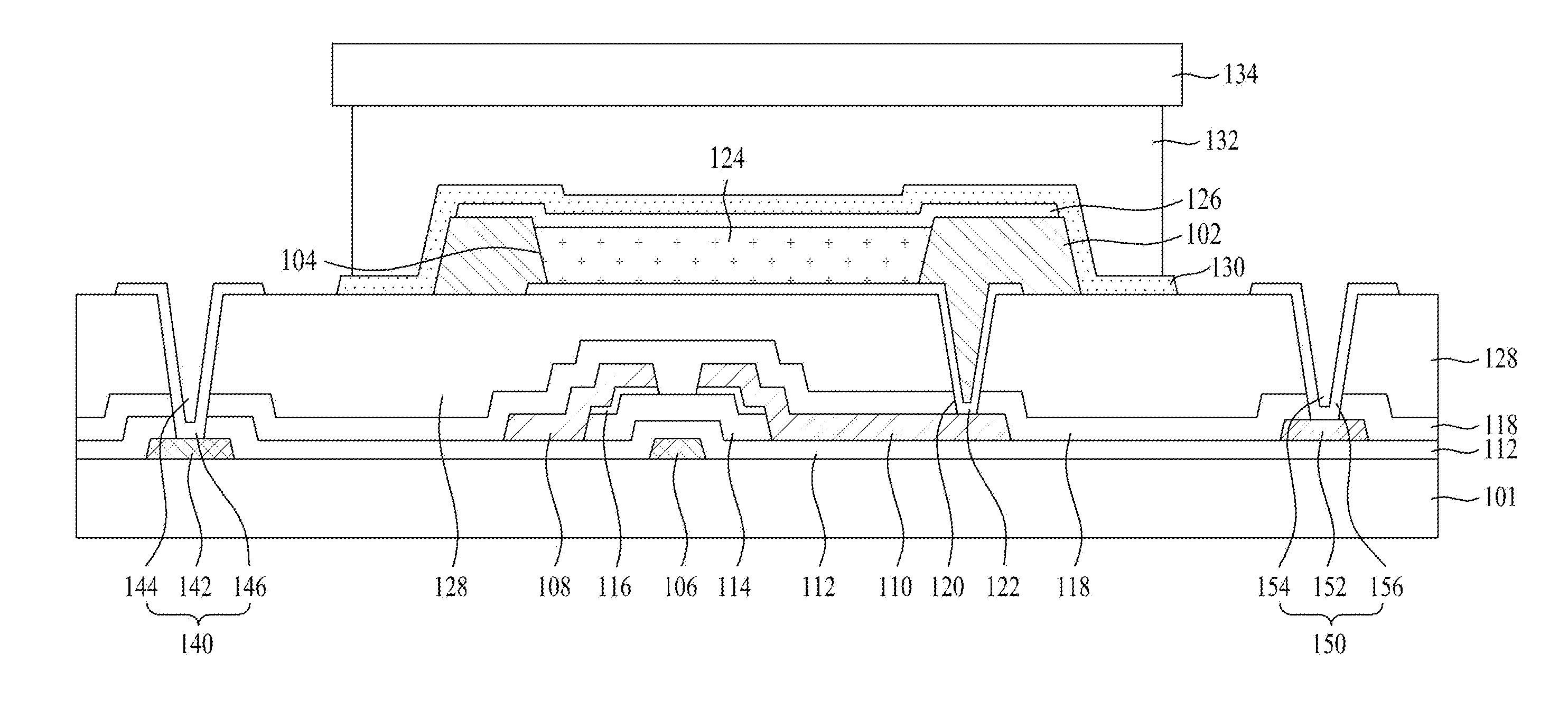
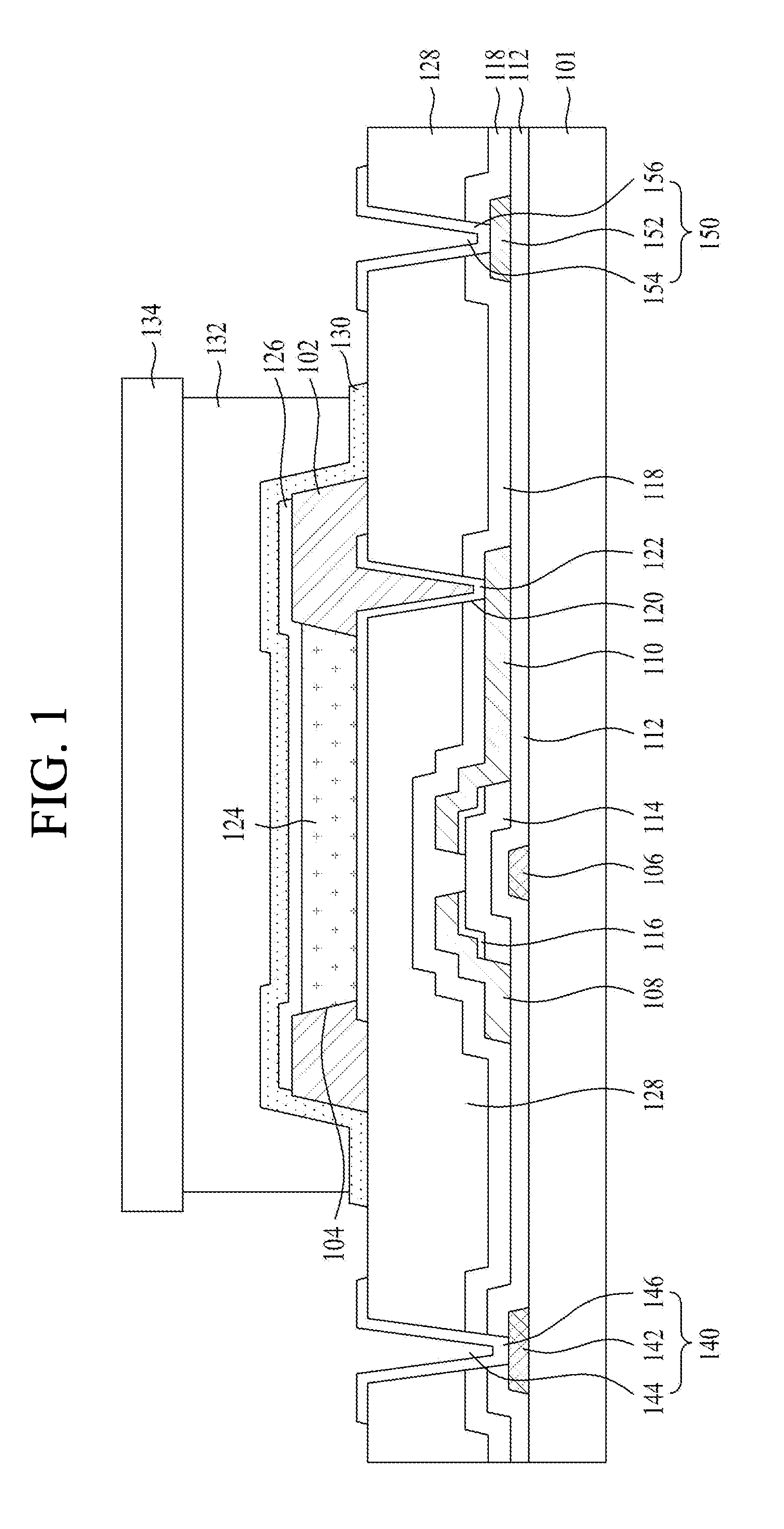
[0029]FIG. 1 is a cross-sectional view illustrating an organic light emitting display panel according to the present invention.

[0030]The organic light emitting display panel illustrated in FIG. 1 includes a light emitting substrate and a sealing substrate 134 adhered to the light emitting substrate via an adhesive film 132.

[0031]The light emitting substrate includes a plurality of thin film transistors formed in a luminescent region of the substrate, light emitting cells connected to the thin film transistors, and a protective insulating film 130 formed to protect the light emitting cells.

[0032]Each of the thin film transistors includes a gate electrode 106, a drain electrode 110 connected to a first electro...


PUM


Abstract

A method of manufacturing an organic light emitting display panel forming a protective insulating film in a luminescent region without causing defects in a pattern is disclosed. The method of manufacturing an organic light emitting display panel includes forming a substrate having a luminescent region and a pad region, simultaneously forming a light emitting cell in the luminescent region and an organic pattern in the pad region, forming a protective insulating film over the substrate, bonding the substrate provided with the protective insulating film and the sealing substrate using an adhesive film formed in a region corresponding to the luminescent region, cutting the bonded substrate provided with the protective insulating film and the sealing substrate into a plurality of unit panels to expose the pad region, and removing the protective insulating film and the organic pattern in the exposed pad region.

Description

CROSS REFERENCE TO RELATED APPLICATIONS[0001]This application claims the benefit of Korean Patent Application No. 10-2012-0054091, filed on May 22, 2012, which is hereby incorporated by reference in its entirety.BACKGROUND OF THE INVENTION[0002]1. Field of the Invention[0003]The present invention relates to a method of manufacturing an organic light emitting display panel capable of forming a protective insulating film in a luminescent region without causing defects in a pattern.[0004]2. Discussion of the Related Art[0005]In recent years, a variety of flat panel display devices having reduced weight and volume, which are drawbacks of cathode ray tubes (CRTs), have been introduced. Examples of flat panel display devices include liquid crystal displays (LCDs), field emission displays (FEDs), plasma display panels (PDPs), and organic electroluminescent displays (ELDs).[0006]Among these display devices, organic electro-luminescent display is a self-emitting device having advantages such...

Claims


Application Information

Patent Timeline
Patent Type & Authority Applications(United States)
IPC IPC(8): H01L51/56
CPCH01L51/56H10K59/131H10K71/851H10K71/421H10K59/873H10K59/871H05B33/04H10K71/00H10K50/841H10K50/844
Inventor YU, HUI-SEONGLEE, SUNG-HOLIM, HYUN-TAEKKIM, IN-SEOKYOO, MYUNG-JAE
Owner LG DISPLAY CO LTD
Features
  • R&D
  • Intellectual Property
  • Life Sciences
  • Materials
  • Tech Scout
  • Unparalleled Data Quality
  • Higher Quality Content
  • 60% Fewer Hallucinations
Learn More