

Memory bandwidth aggregation using simultaneous access of stacked semiconductor memory die
a technology of memory bandwidth and semiconductor memory die, which is applied in the field of memory bandwidth aggregation using simultaneous access of stacked semiconductor memory die, can solve the problems of significant engineering challenges and increased die size of through-die via in the stack of dies
- Summary
- Abstract
- Description
- Claims
- Application Information
AI Technical Summary
Benefits of technology
Problems solved by technology
Method used
Image

Examples
Embodiment Construction
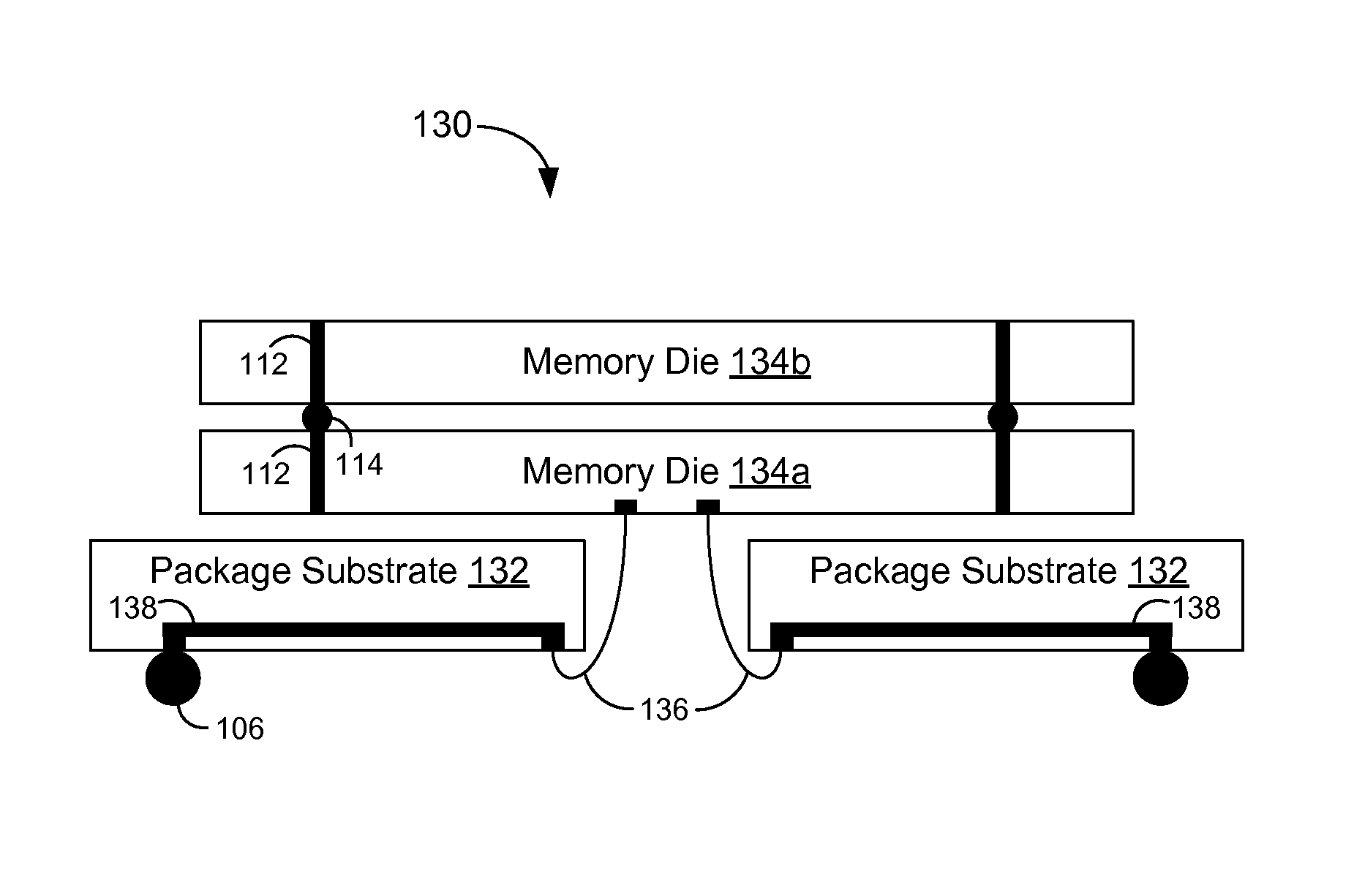
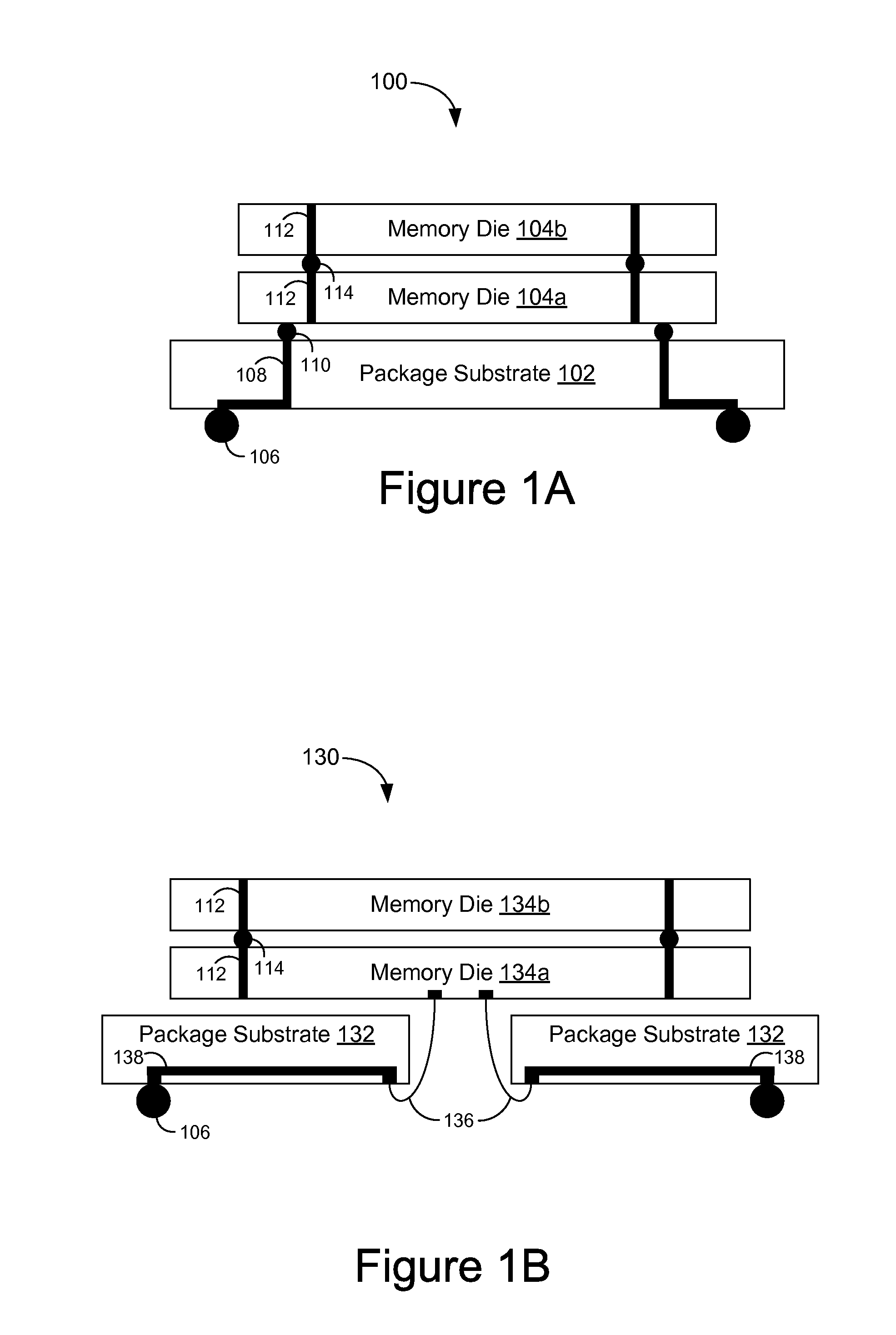
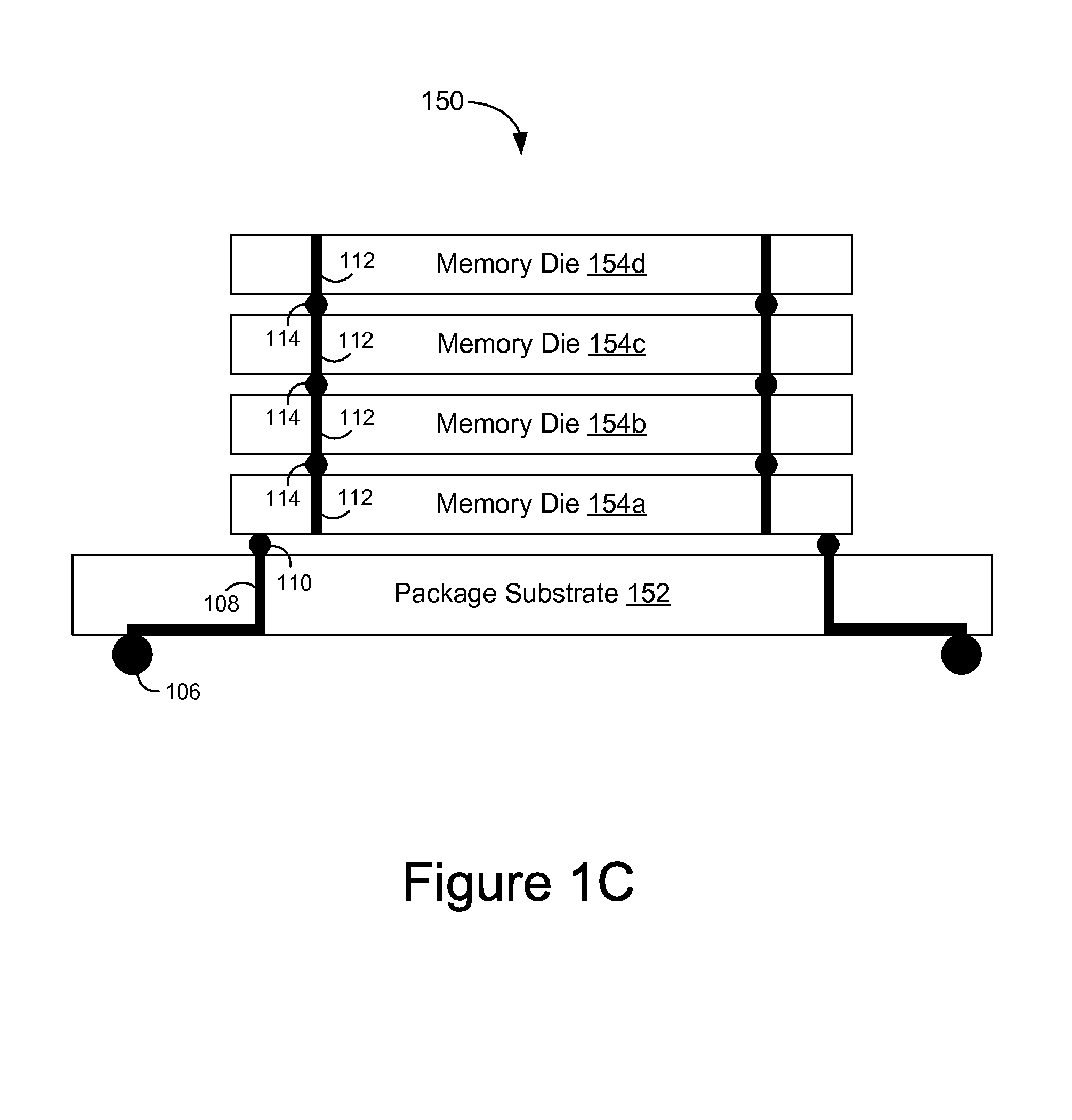
[0016]Embodiments are disclosed in which data accessed from multiple memory die arranged in a stacked configuration is aggregated.
[0017]In some embodiments, a packaged semiconductor memory device includes a data pin, a first memory die, and a second memory die. The first memory die includes a first data interface coupled to the data pin and a first memory core having a plurality of banks. The second memory die is stacked with the first memory die and includes a second memory core having a plurality of banks. A respective bank of the first memory core and a respective bank of the second memory core are configured to perform memory access operations in parallel, and the first data interface is configured to provide aggregated data from the parallel memory access operations. For example, the respective banks of the first and second memory cores are configured to perform parallel row access operations in response to a first command signal and parallel column access operations in respons...
PUM
 Abstract
Description
Claims
Application Information