
Key membrane and electronic device using the same

a key membrane and electronic device technology, applied in the field of electronic devices, can solve the problems of reducing the touch sensation of the key, increasing the difficulty of pasting operation of the conductive portion, and single insulating membranes not being able to synchronize the improvement of pasting operation and touching sensation

Inactive Publication Date: 2013-12-26
HONG FU JIN PRECISION IND (SHENZHEN) CO LTD +1
View PDF2 Cites 2 Cited by
  • Summary
  • Abstract
  • Description
  • Claims
  • Application Information

AI Technical Summary

Benefits of technology

The patent text discusses how electronic devices, such as DVD players, have a key portion with keys and a printed circuit board (PCB). A single insulating membrane is placed between the key portion and the PCB and includes conductive portions that correspond to the keys. The membrane covers the PCB and the conductive portions are placed on the surface of the membrane facing the PCB. However, changes in the thickness of the membrane can impact the touch sensation and make it harder or easier to place the conductive portion, leading to limitations in optimizing touch sensation and pasting efficiency. The technical effect of the patent is to provide an improved solution for improving the pasting operation and touching sensation of the electronic device.

Problems solved by technology

However, when the single insulating membrane becomes thinner, the touching sensation of the electronic device improves, but the pasting operation of the conductive portion becomes more difficult; when the single insulating membrane becomes thicker, the touching sensation of the key is reduced, but the pasting operation of the conductive portion improves.
Thus, the single insulating membrane cannot synchronously improve the pasting operation and the touching sensation.

Method used


Image

  • Key membrane and electronic device using the same
  • Key membrane and electronic device using the same
  • Key membrane and electronic device using the same

Examples


Embodiment Construction

[0011]Embodiments of the present disclosure will be described in detail with reference to the drawings.

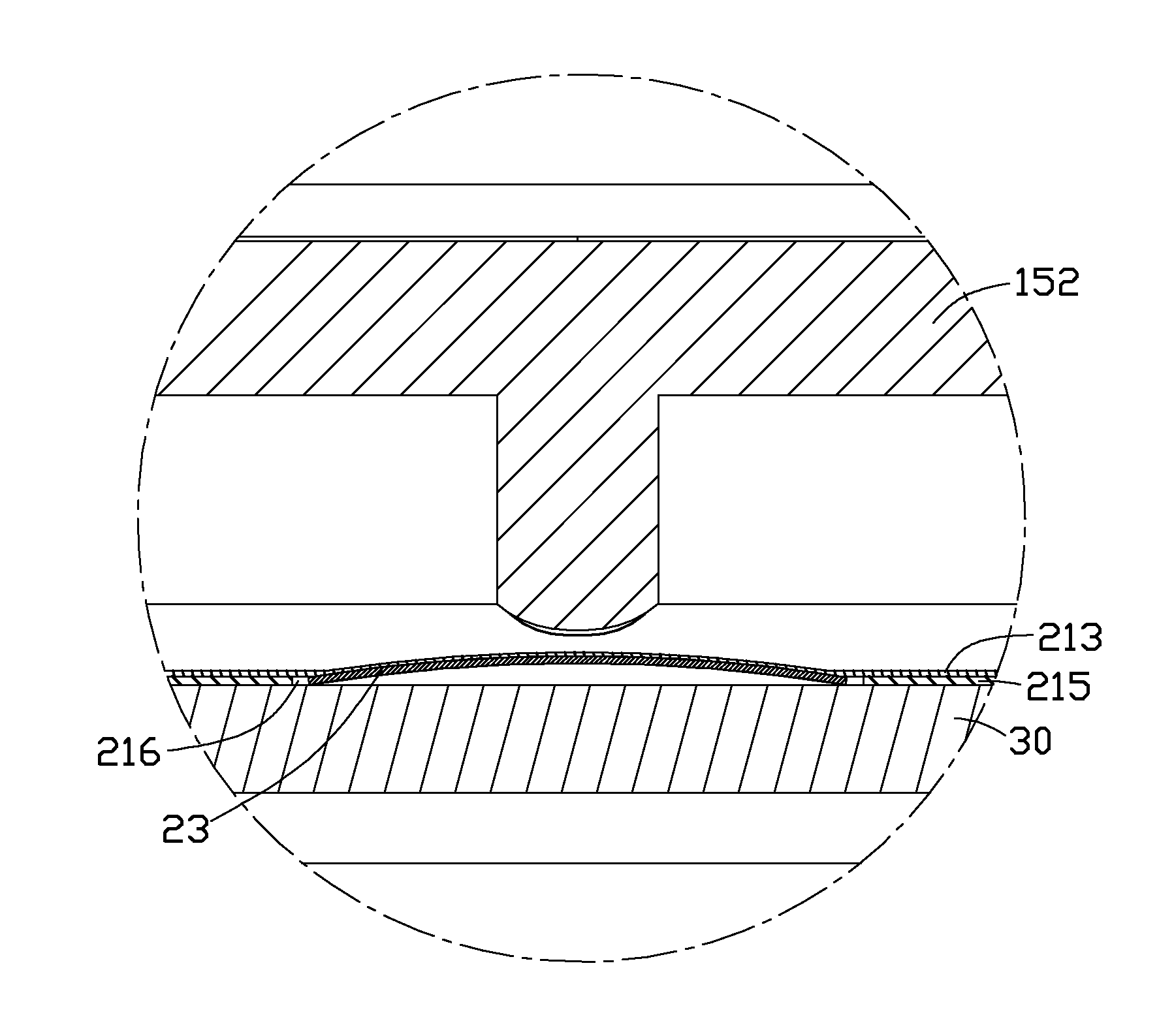
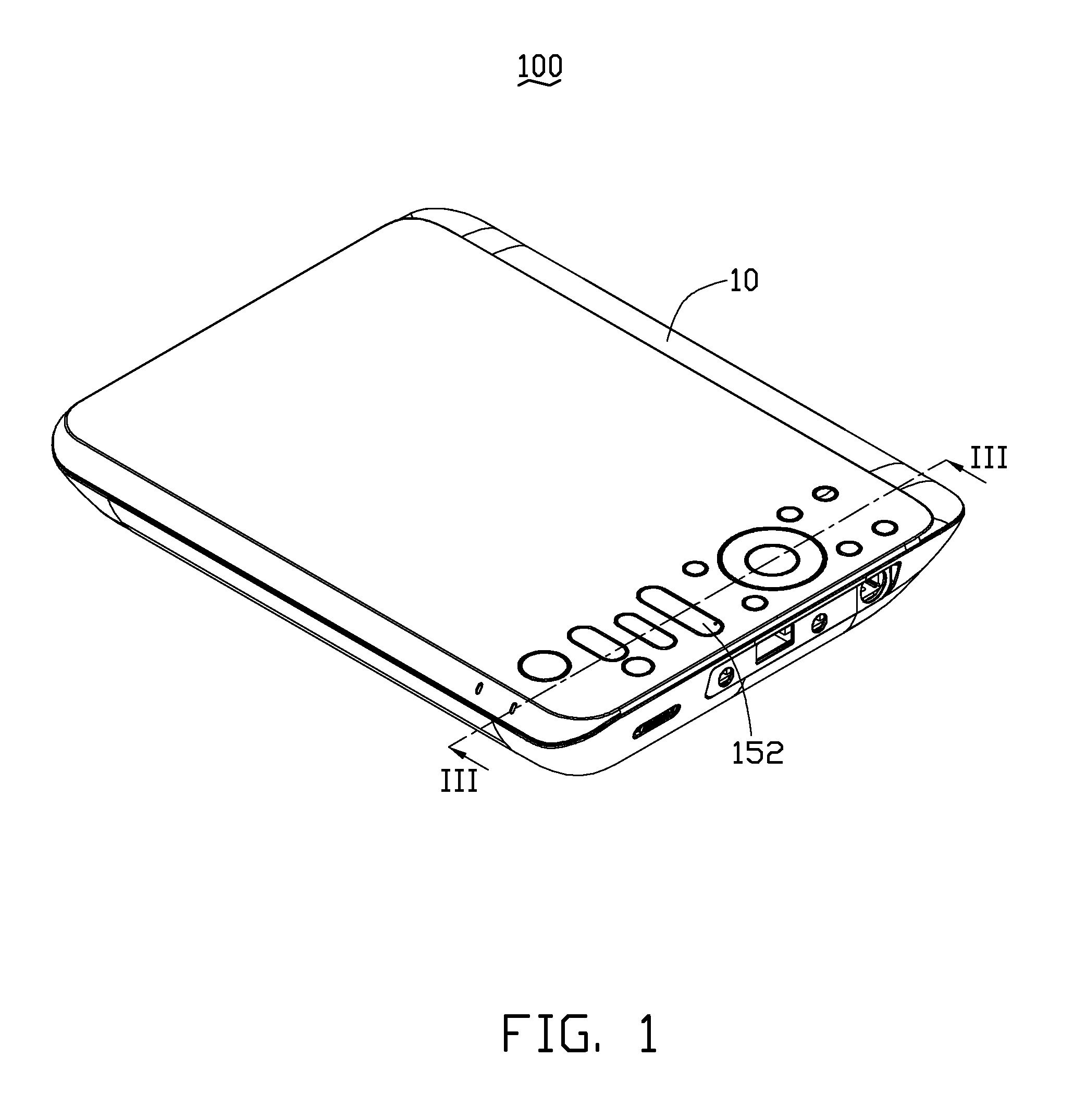
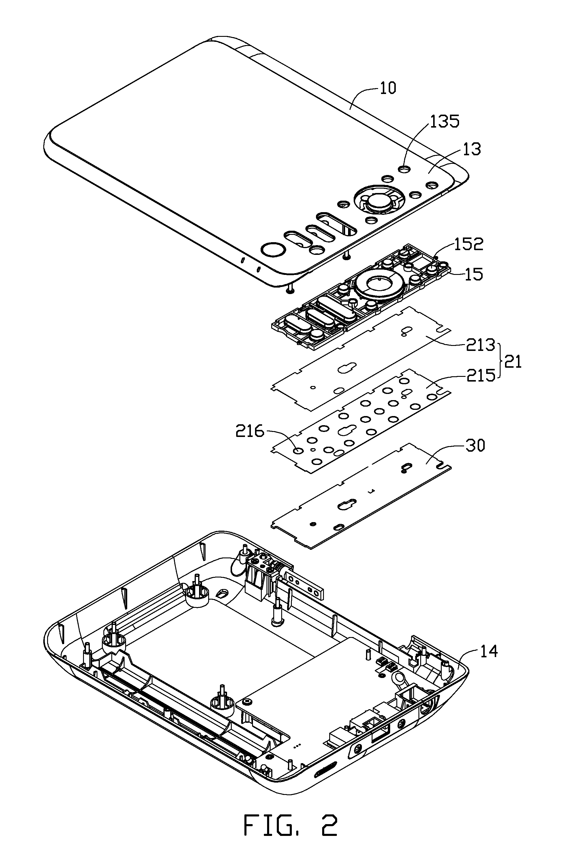
[0012]FIGS. 1 and 2 show an electronic device 100 of the embodiment. The electronic device 100 includes a housing 10, a key membrane 20 (as shown in FIG. 3), and a printed circuit board (PCB) 30. The key membrane 20 covers the PCB 30, and is used for establishing an electrical connection with the PCB 30. The key membrane 20 is deformable when being pressed, and the PCB 30 generates a corresponding control signal when the key membrane 20 is deformed. In the embodiment, the electronic device 100 is a portable DVD player.

[0013]The housing 10 includes an upper cover 12 (as shown in FIG. 3), a bottom cover 14. The upper cover 12 cooperates with the bottom cover 14 to form a closed space (not labeled) for receiving the key membrane 20, the PCB 30, and other electronic components (not shown), such as an optical reading head. The upper cover 12 is substantially rectangular and includes a k...


PUM


Abstract

An electronic device comprises a housing, a printed circuit board (PCB) received in the housing, and a key membrane covered on the PCB. The housing comprises a key portion with a plurality of keys. The key membrane comprises a first insulating layer and a second insulating layer covered by the first insulating layer. The second insulating layer is mounted on the PCB and defines a plurality of through holes. The through holes correspond to the plurality of keys in a one-to-one relationship. When one of the plurality of keys is being pressed, a part of the first insulating layer corresponding to the pressed key is deformed and establishes the electrical connection with the PCB, thus the PCB is actuated to generate a corresponding control signal.

Description

BACKGROUND[0001]1. Technical Field[0002]The present disclosure relates to electronic devices, and more particularly relates to an electronic device with a key membrane.[0003]2. Description of Related Art[0004]Electronic devices, such as DVD players, include a key portion with a plurality of keys, a printed circuit board (PCB), and a key membrane set between the key portion and the PCB. The key membrane is a single insulating membrane and includes a plurality of conductive portions corresponding to the keys. The single insulating membrane covers on the PCB. The conductive portions are pasted on the surface of the single insulating membrane facing the PCB. However, when the single insulating membrane becomes thinner, the touching sensation of the electronic device improves, but the pasting operation of the conductive portion becomes more difficult; when the single insulating membrane becomes thicker, the touching sensation of the key is reduced, but the pasting operation of the conduc...

Claims


Application Information

Patent Timeline
Patent Type & Authority Applications(United States)
IPC IPC(8): H01H13/704
CPCH01H13/704H01H2205/032H01H2221/05H01H2223/036H01H2233/002H01H2227/004
Inventor YU, YONG-JUNWAN, XUE-FENGYANG, FAN
Owner HONG FU JIN PRECISION IND (SHENZHEN) CO LTD
Learn More