Vcsel array with increased efficiency

Active Publication Date: 2013-12-26
TRUMPF PHOTONIC COMPONENTS GMBH
View PDF2 Cites 5 Cited by
  • Summary
  • Abstract
  • Description
  • Claims
  • Application Information

AI Technical Summary

Benefits of technology

[0009]With this measure, the substrate still can be used for carrier injection into the active region although an undoped semiconductor mirror is arranged between the

Problems solved by technology

This requires an electrically conducting (doped) bottom DBR, which then on the other hand h

Method used


Image

  • Vcsel array with increased efficiency
  • Vcsel array with increased efficiency
  • Vcsel array with increased efficiency

Examples


Embodiment Construction

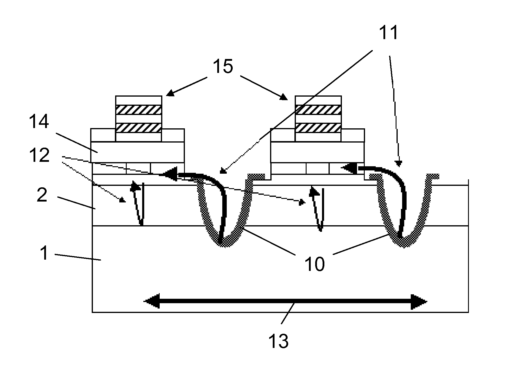
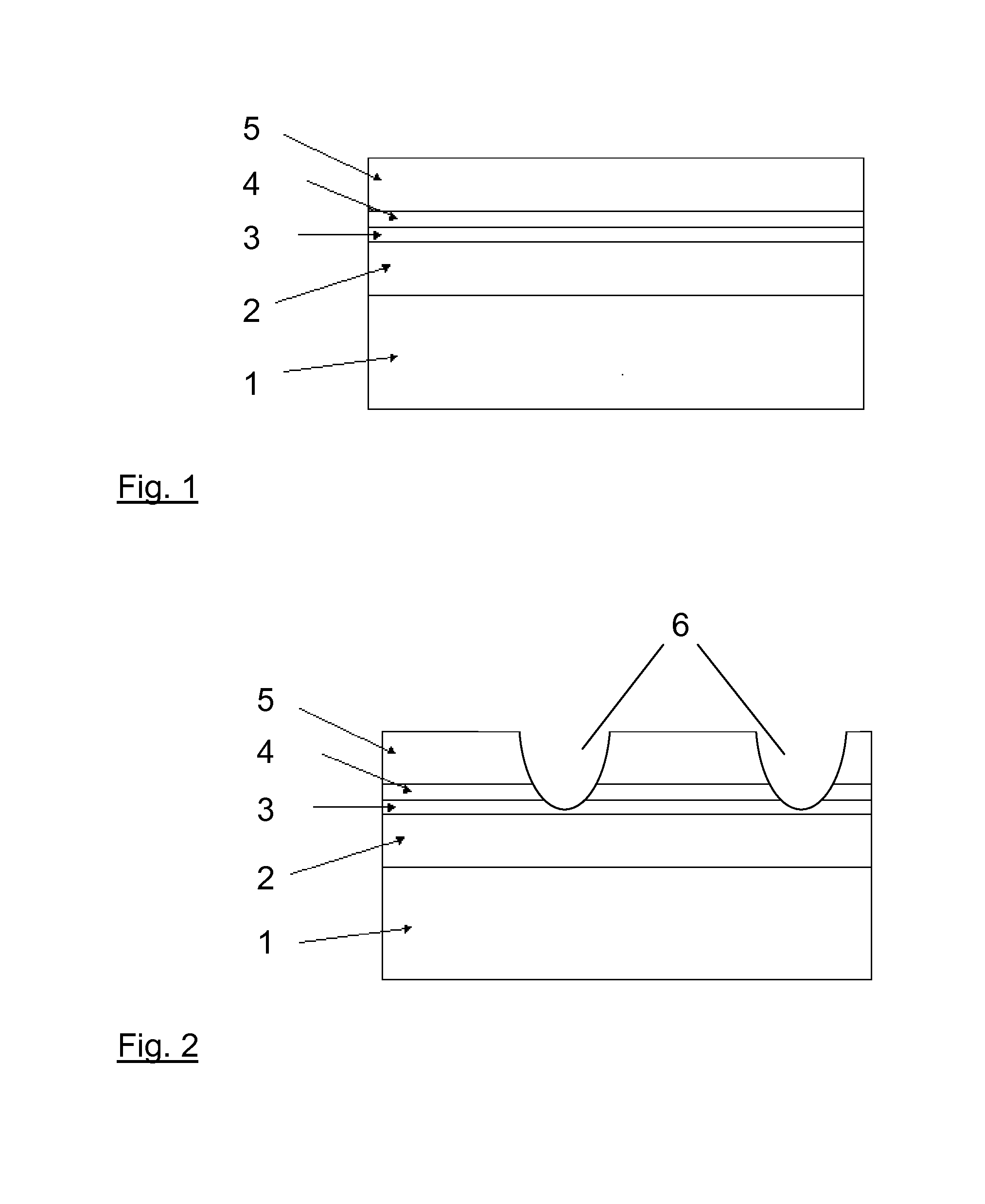
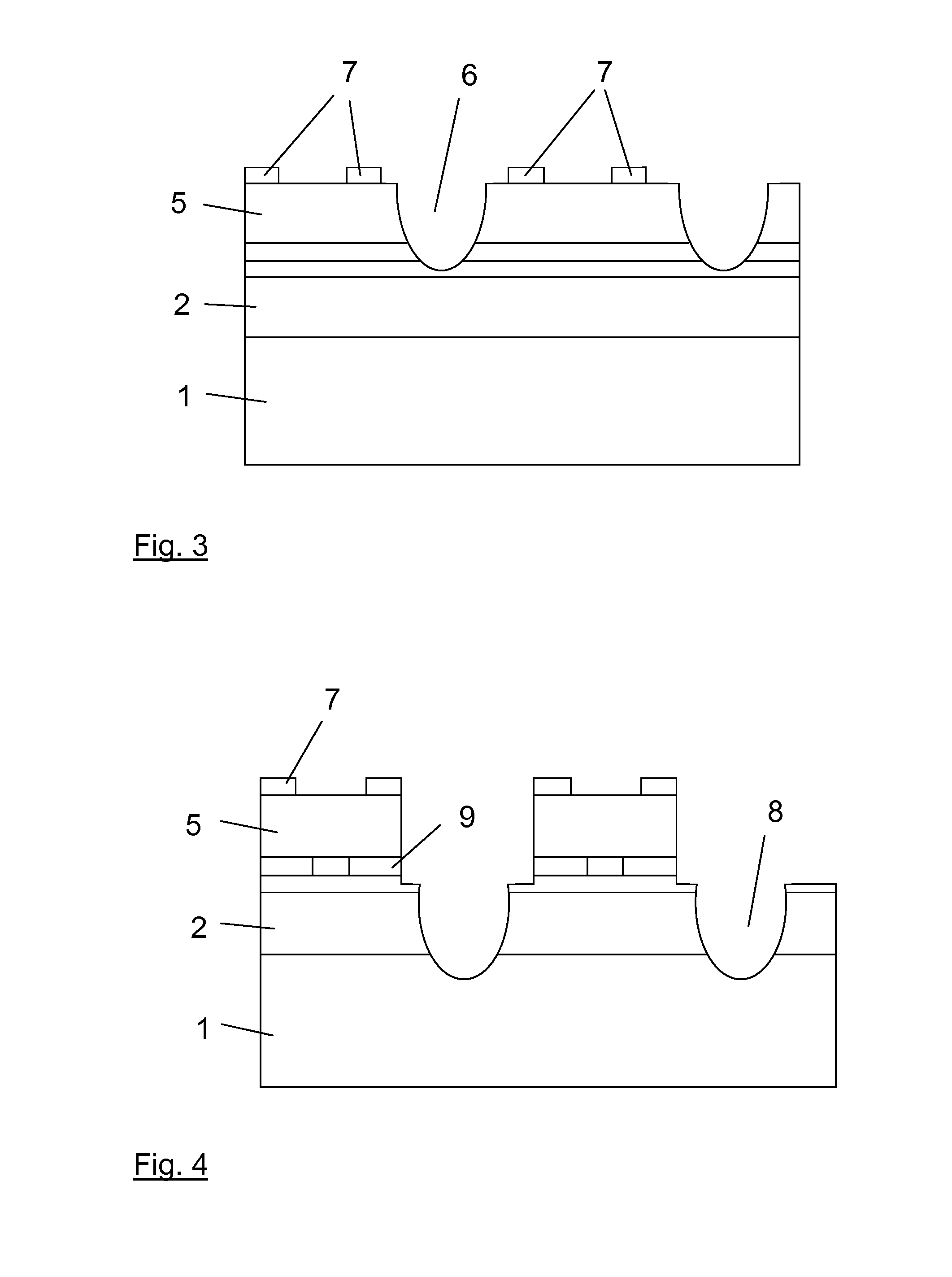
[0021]The figures show an example for fabricating a VCSEL array according to the present invention. In the figures, only a part of the array with two single VCSELs is shown. It is clear that the complete array as a higher number of VCSELs which are fabricated with the same process steps at the same time.

[0022]The VCSELs of the proposed array can be fabricated in the known manner by epitaxially growing a layer stack on a carrier substrate or wafer. FIG. 1 shows an example for such an epitaxial layer stack comprising an undoped DBR 2, a n-doped current injection layer 3, an active layer 4 and a p-doped DBR 5 on the top side. The materials for the single layers as well as the configuration of the DBRs and the active layer can be chosen as already known in the art.

[0023]The epitaxial layer stack of FIG. 1 is then subjected to a wet chemical etch at the wafer areas that will later serve as electrical connections. The trenches 6 formed by this wet chemical etch are indicated in FIG. 2. Th...


PUM


Abstract

The present invention relates to a VCSEL array comprising several VCSELs arranged side by side on a common substrate (1). Each VCSEL is formed of at least a top mirror (5, 14), an active region (4), a current injection layer (3) and an undoped bottom semiconductor mirror (2). The current injection layer (3) is arranged between the active region (4) and the bottom semiconductor mirror (2). At least an upper layer of the substrate (1) is electrically conducting. Trenches (8) and/or holes are formed between the bottom semiconductor mirrors (2) of said VCSELs to said upper layer of said substrate (1). A metallization (9) electrically connects the upper layer of the substrate (1) with the current injection layer (3) through said trenches (8) and/or holes. The proposed VCSEL array allows a homogeneous current injection an has a high efficiency and power density.

Description

FIELD OF THE INVENTION[0001]The present invention relates to an array comprising several vertical cavity surface emitting lasers (VCSEL) arranged side by side on a common substrate, each VCSEL being formed of at least a top mirror, an active region, a current injection layer and an undoped bottom semiconductor mirror, said current injection layer being arranged between said active region and said bottom semiconductor mirror. Such a VCSEL array can be used in applications requiring semiconductor light sources with high power density, for example in lighting applications.BACKGROUND OF THE INVENTION[0002]High efficient VCSELs require highly reflective semiconductor mirrors, typically realised as distributed Bragg reflectors (DBR). Doped DBRs show a higher absorption of the generated laser light than undoped DBRs. Therefore, for high efficient VCSEL designs the use of undoped DBRs is preferred.[0003]R. C. Strijbos et al., “Current crowding in oxide-confined intracavity-contacted VCSELs”...

Claims


Application Information

Patent Timeline
IPC IPC(8): H01S5/42
CPCH01S5/423H01S5/0207H01S5/18311H01S5/18341H01S5/18344H01S5/18361H01S5/18369H01S5/2081
Inventor GERLACH, PHILIPP HENNING
Owner TRUMPF PHOTONIC COMPONENTS GMBH
Why Eureka
Try Eureka