Die Attach Pick Error Detection

a technology of error detection and die attachment, applied in the field of semiconductor processing systems, can solve problems such as general undetectable results

Active Publication Date: 2014-01-02
TEXAS INSTR INC
View PDF2 Cites 15 Cited by
  • Summary
  • Abstract
  • Description
  • Claims
  • Application Information

AI Technical Summary

Problems solved by technology

Any error that occurs after reference die alignment is complete is g...

Method used


Image

  • Die Attach Pick Error Detection
  • Die Attach Pick Error Detection
  • Die Attach Pick Error Detection

Examples


Embodiment Construction

[0016]Specific embodiments of the invention will now be described in detail with reference to the accompanying figures. Like elements in the various figures are denoted by like reference numerals for consistency. In the following detailed description of embodiments of the invention, numerous specific details are set forth in order to provide a more thorough understanding of the invention. However, it will be apparent to one of ordinary skill in the art that the invention may be practiced without these specific details. In other instances, well-known features have not been described in detail to avoid unnecessarily complicating the description.

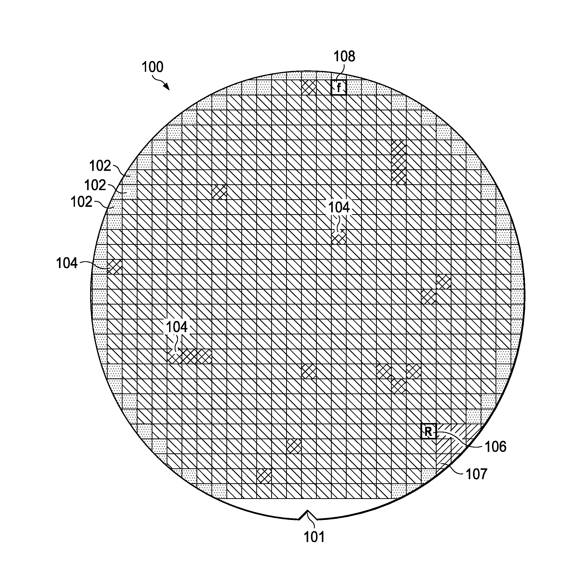
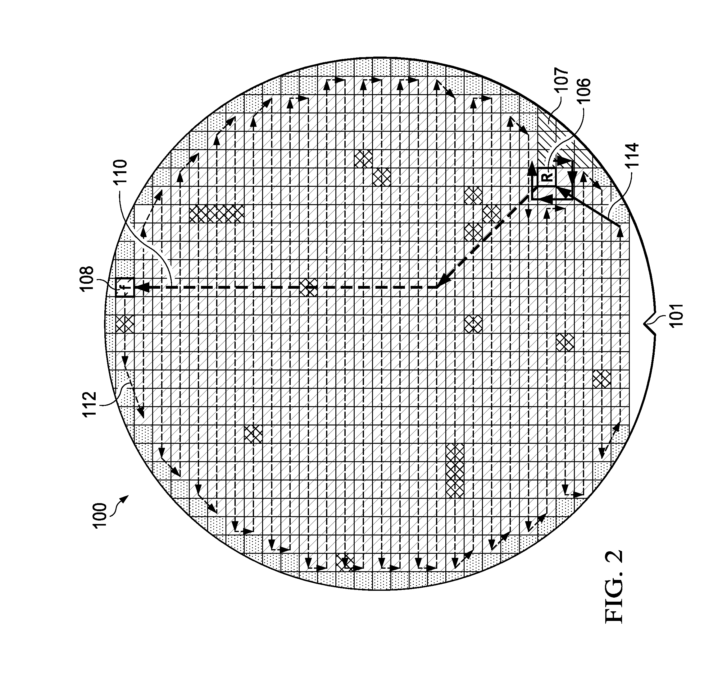
[0017]Embodiments of the invention are directed, in general, to processing semiconductor wafers and, more particularly, to detecting pick & place index and map shift issues in normal wafer processing. Embodiments of the invention now will be described more fully hereinafter with reference to the accompanying drawings. This invention may, howeve...


PUM


Abstract

Embodiments of the invention provide a method to detect pick and place indexing errors on each manufacturing batch (lot) of semiconductor wafer processed during a die attach process using a preselected skeleton of check die. The known locations of the check skeleton die are verified during picking of die from the wafer. If the check skeleton cannot be correctly verified at the known locations, then a pick error is indicated. The embodiments may be implemented on existing die attach equipment.

Description

CLAIM OF PRIORITY UNDER 35 U.S.C. 119(e)[0001]The present application claims priority to and incorporates by reference U.S. Provisional Application No. 61 / 665,392, (attorney docket TI-72466S) filed Jun. 28, 2012, entitled “Method for Die Attach Pick Error Detection.” The present application also claims priority to and incorporates by reference U.S. Provisional Application No. 61 / 664,829, (attorney docket TI-72559PS) filed Jun. 27, 2012, entitled “Detection Using Pick & Place Index Map and Map Shift”.FIELD OF THE INVENTION[0002]Embodiments of the invention are directed, in general, to semiconductor processing systems and more specifically to die attachment and pick error detectionBACKGROUND OF THE INVENTION[0003]A conventional semiconductor (e.g., silicon) wafer contains a plurality of integrated circuit die, also referred to as chips. Conventional assembly processes such as pick and place use an electronic wafer map that includes information indicative of die attributes such as the ...

Claims


Application Information

Patent Timeline
IPC IPC(8): G01R31/3185
CPCG01R31/318511G01R31/2831H01L2924/0002H01L2924/00H01L22/30H01L23/544H01L2223/54493
Inventor OHMART, DALESUBRAMANIAN, BALAMURUGANLEANO, RENATO HERACLEO ORDUNADIPASUPIL, SONNY EVANGELISTAPERALTA, RONALD JAY V.
Owner TEXAS INSTR INC
Why Eureka
Try Eureka