Check patentability & draft patents in minutes with Patsnap Eureka AI!

Transient Voltage Suppressor Circuit, and Diode Device Therefor and Manufacturing Method Thereof

a technology of transient voltage and suppressor, which is applied in the direction of diodes, semiconductor devices, electrical apparatus, etc., can solve the problems of high parasitic capacitance, reduced current which the tvs circuit can sustain, and limited application range of the tvs circuit b>1/b>

Active Publication Date: 2014-01-16
RICHTEK TECH
View PDF1 Cites 2 Cited by
  • Summary
  • Abstract
  • Description
  • Claims
  • Application Information

AI Technical Summary

Benefits of technology

The present invention provides a TVS circuit with a diode device that can sustain a higher forward current, and a manufacturing method thereof. This is achieved by providing a TVS circuit with a suppressor device and at least one diode device that has a PN junction in a reverse direction to the suppressor device. The diode device has a high impurity concentration in the PN junction, which reduces parasitic capacitance and allows for faster operation of the protected circuit. This allows for a broader application range of the protected circuit.

Problems solved by technology

Because the suppressor device S1 needs to release a high current in a very short time, a large area PN junction is required, resulting in a very high parasitic capacitance.
And if the TVS circuit 1 has a lower capacitance, the current which the TVS circuit can sustain is reduced, and thus the application range of the TVS circuit 1 is limited.

Method used


Image

  • Transient Voltage Suppressor Circuit, and Diode Device Therefor and Manufacturing Method Thereof
  • Transient Voltage Suppressor Circuit, and Diode Device Therefor and Manufacturing Method Thereof
  • Transient Voltage Suppressor Circuit, and Diode Device Therefor and Manufacturing Method Thereof

Examples


Embodiment Construction

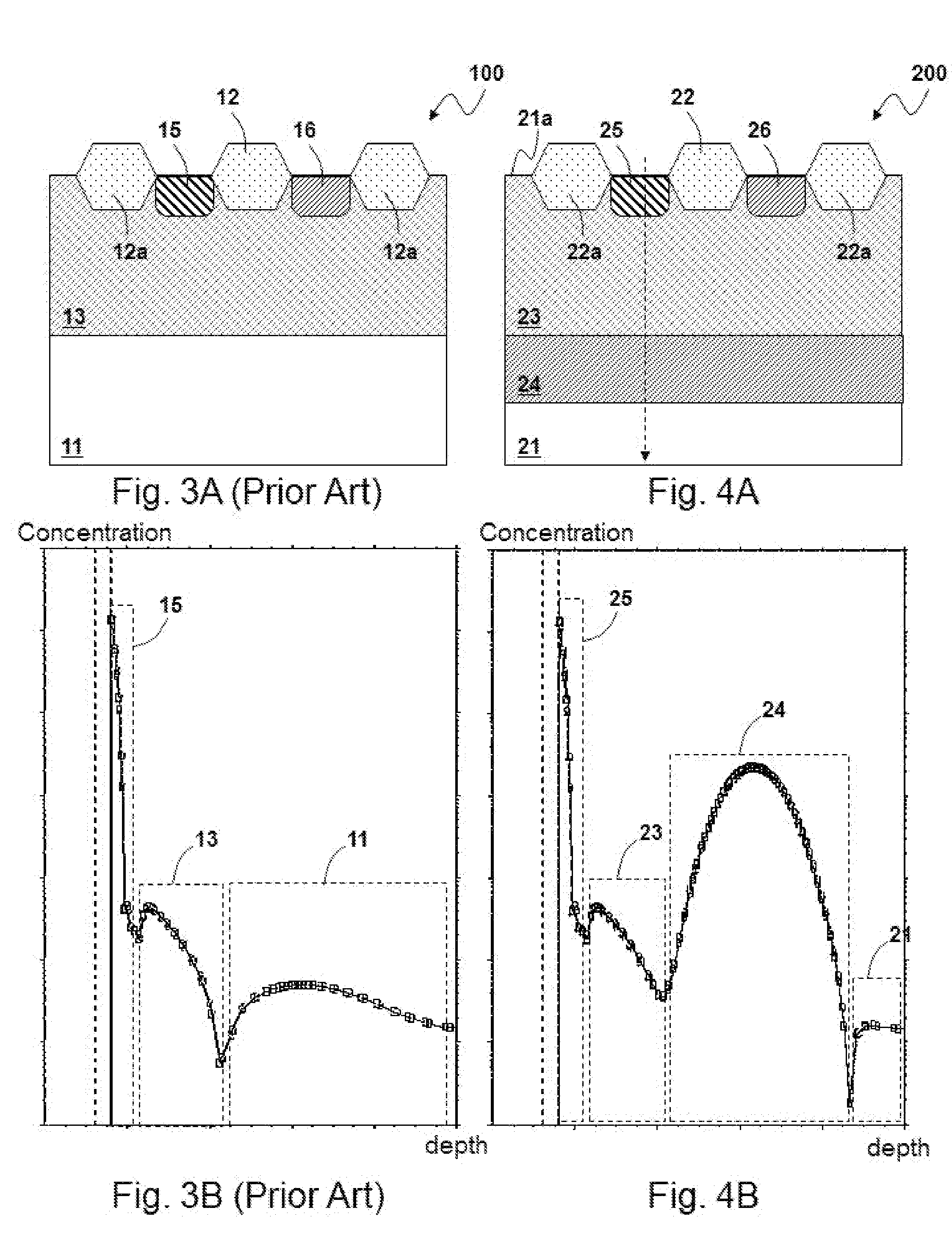
[0029]The drawings as referred to throughout the description of the present invention are for illustration only, to show the interrelations between the regions and the process steps, but not drawn according to actual scale.

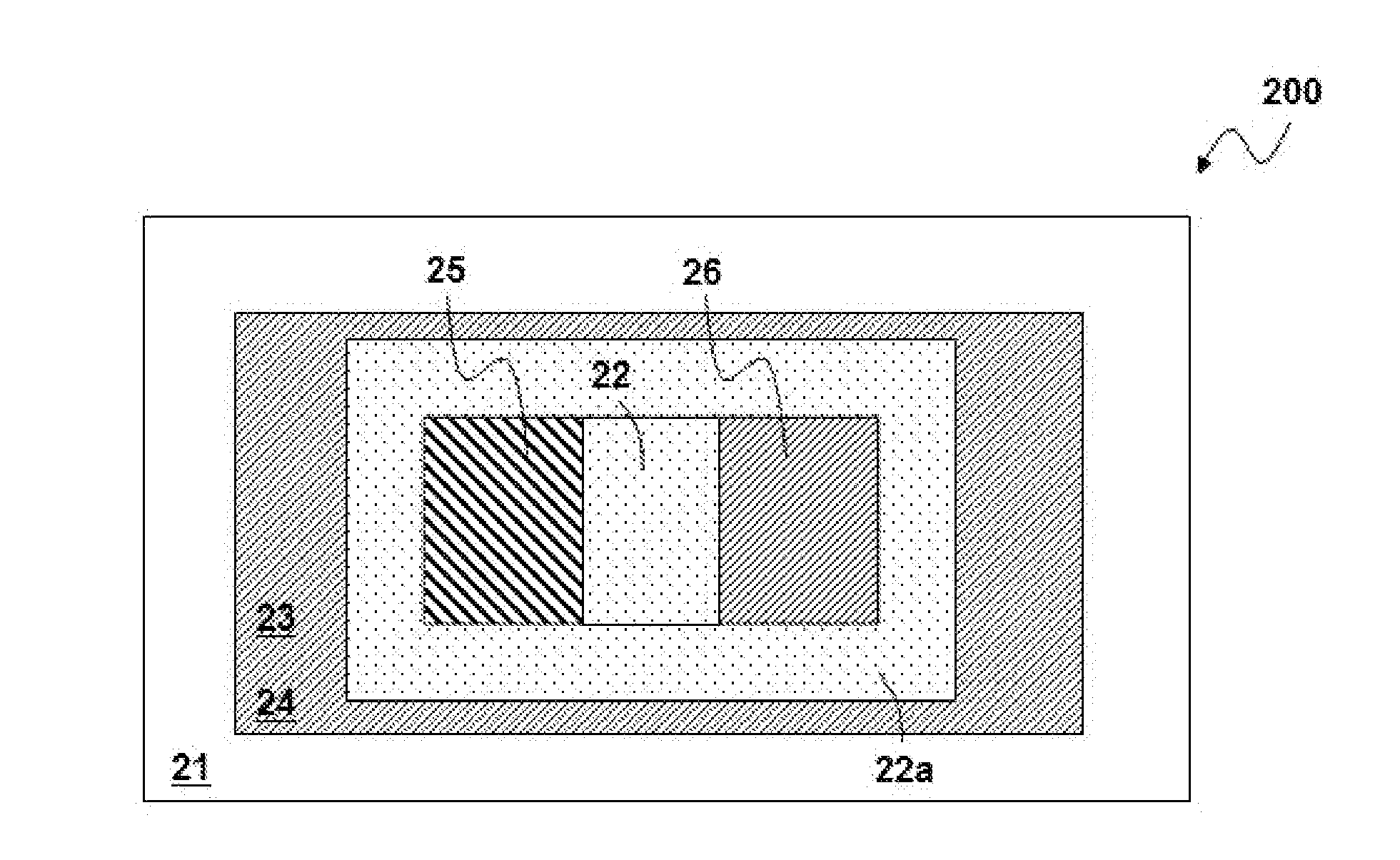
[0030]Please refer to FIGS. 4A and 4B for a first embodiment according to the present invention, wherein FIG. 4A is a cross-section schematic diagram showing a diode device 200 for a transient voltage suppressor (TVS) circuit according to the present invention. As shown in FIG. 4A, the diode device 200 is formed in a substrate 21 which has an upper surface 21a, wherein the substrate 21 is for example but not limited to a P-type substrate (or an N-type substrate in another embodiment). Next, for example but not limited to an N-type well 23 is formed beneath the upper surface 21a in the substrate 21, and a buried layer 24 is formed beneath the well 23 in the substrate 21. The buried layer 24 has a same conductive type with the well 23 (N-type in this embodiment), an...


PUM


Abstract

The present invention discloses a transient voltage suppressor (TVS) circuit, and a diode device therefor and a manufacturing method thereof. The TVS circuit is for coupling to a protected circuit to limit amplitude of a transient voltage which is inputted to the protected circuit. The TVS circuit includes a suppressor device and at least a diode device. The diode device is formed in a substrate, which includes: a well formed in the substrate; a separation region formed beneath the upper surface; a anode region and a cathode region, which are formed at two sides of the separation region beneath the upper surface respectively, wherein the anode region and the cathode region are separated by the separation region; and a buried layer, which is formed in the substrate below the well with a higher impurity density and a same conductive type as the well.

Description

BACKGROUND OF THE INVENTION[0001]1. Field of Invention[0002]The present invention relates to a transient voltage suppressor (TVS) circuit, and a diode device therefor and a manufacturing method thereof; particularly, it relates to such TVS circuit wherein a higher forward current can be sustained, and a diode device therefor and a manufacturing method thereof.[0003]2. Description of Related Art[0004]FIG. 1A shows a typical TVS circuit 1. The TVS circuit 1 is coupled to a protected circuit 2, for limiting amplitude of a transient voltage from an input / output (I / O) pad 3, so as to protect the protected circuit 2 from damages caused by the transient voltage (by static charges, for example). In general, the TVS circuit 1 includes a suppressor device S1 for clamping the amplitude of the transient voltage and for absorbing an excess current path. Because the suppressor device S1 needs to release a high current in a very short time, a large area PN junction is required, resulting in a very...

Claims


Application Information

Patent Timeline
IPC IPC(8): H01L27/06H01L21/82
CPCH01L27/0814H01L27/0255H01L21/265H01L21/76224H01L29/0649H01L29/66136
Inventor HUANG, TSUNG-YISU, JIN-LIAN
Owner RICHTEK TECH
Features
  • R&D
  • Intellectual Property
  • Life Sciences
  • Materials
  • Tech Scout
  • Unparalleled Data Quality
  • Higher Quality Content
  • 60% Fewer Hallucinations
Learn More