Wafer container

a container and semiconductor technology, applied in the field of container for the transportation of semiconductor wafers, can solve the problems of not being integrated with the enclosure, unable to meet the intended purpose of the wafer, and being susceptible to damage, so as to reduce the amount of radial wafer shift, and increase the ability of the wafer containment device to protect semiconductor wafers.

Inactive Publication Date: 2014-02-06
TEXCHEM ADVANCED PRODS
View PDF6 Cites 6 Cited by
  • Summary
  • Abstract
  • Description
  • Claims
  • Application Information

AI Technical Summary

Benefits of technology

[0019]It is an object of the semiconductor wafer container to limit the amount of radial movement of the wafer within the container. Limiting radial movement is important because when shipping “bumped” wafers, that are stacked on spacer rings where the rings touch the periphery of the wafer, it will not shift radially into the areas containing the solder bumps. The improvements increase the wafer containment device's ability to protect semiconductor wafers and reduce radial wafer shift for both bumped and non-bumped wafers. This design can be used with or without spacer rings between the wafers in the vertical stack.

Problems solved by technology

The semiconductor wafers are fragile and damage to the surface of the wafers can make the wafer useless for the intended purpose.
Further, the cushion is not integrated with the enclosure and exists as a separate component.
This cushion pushes from only one side and pushes the wafers against an outside wall where they are susceptible to damage.
While the nesting walls provide protection from side impacts they do not provide flexibility to absorb and cushion a side impact or drop.
Damage may also occur if the force is such that the outer wall flexes enough to interfere with the inner wall, thereby damaging the wafers.
That can cause the semiconductor wafers to shift and scratch.
The corrugated inner lip provides multiple surfaces for the edges if the semiconductor wafers to make contact with, but because the edges are corrugated the tangential walls of the corrugation limit the flexing of the inner lips.
Some semiconductor wafer containers use a rotation locking design where the locating mechanism with an exclusive inner surface or exterior surface do not securely capture the wall that they are adjacent to in both directions of rotation.
These deficiencies result in larger gaps between the plus and minus rotational limiting surfaces, thereby leading to more rotational movement.
Prior art designs have left the latch exposed to accidental contact that can open one or more of the latches that holds the two halves of the enclosure together.
The designs all fail to address placing the latch in a well to prevent accidental opening during handling and shipping.
These designs have several drawbacks including but not limited to the parts not being rigid with respect to the bottom assembly because they must be sonic welded, bonded or snapped together and that secondary parts or assembly operations are more expensive to produce.
The engagement of latches that secure the top and bottom housings together have a number of limitations.
The raise straight sloped surface is susceptible to damage.
Moreover, the straight slope does not provide an ideal self gripping to engage between the top and bottom housings.

Method used


Image

  • Wafer container
  • Wafer container
  • Wafer container

Examples


Embodiment Construction

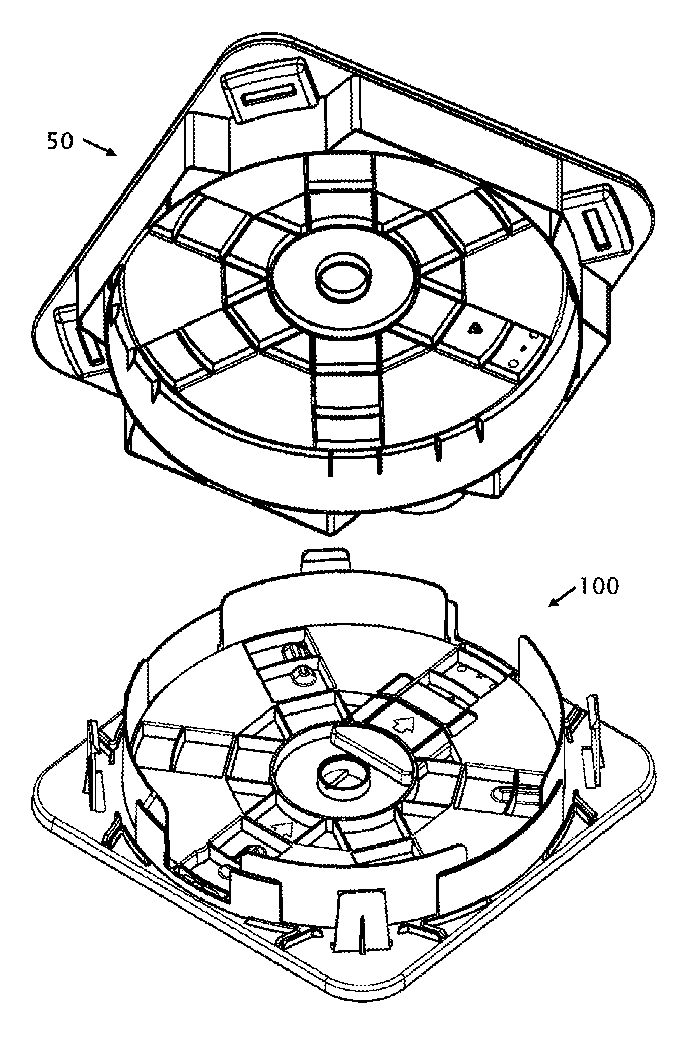
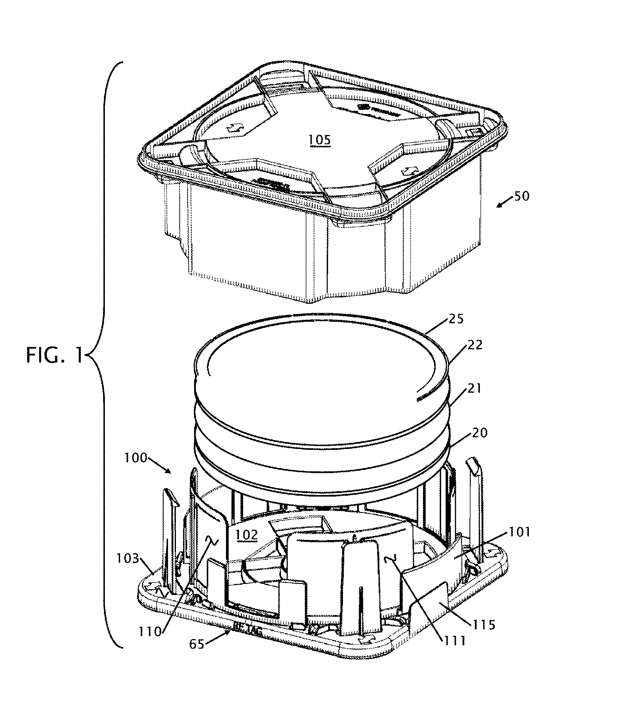
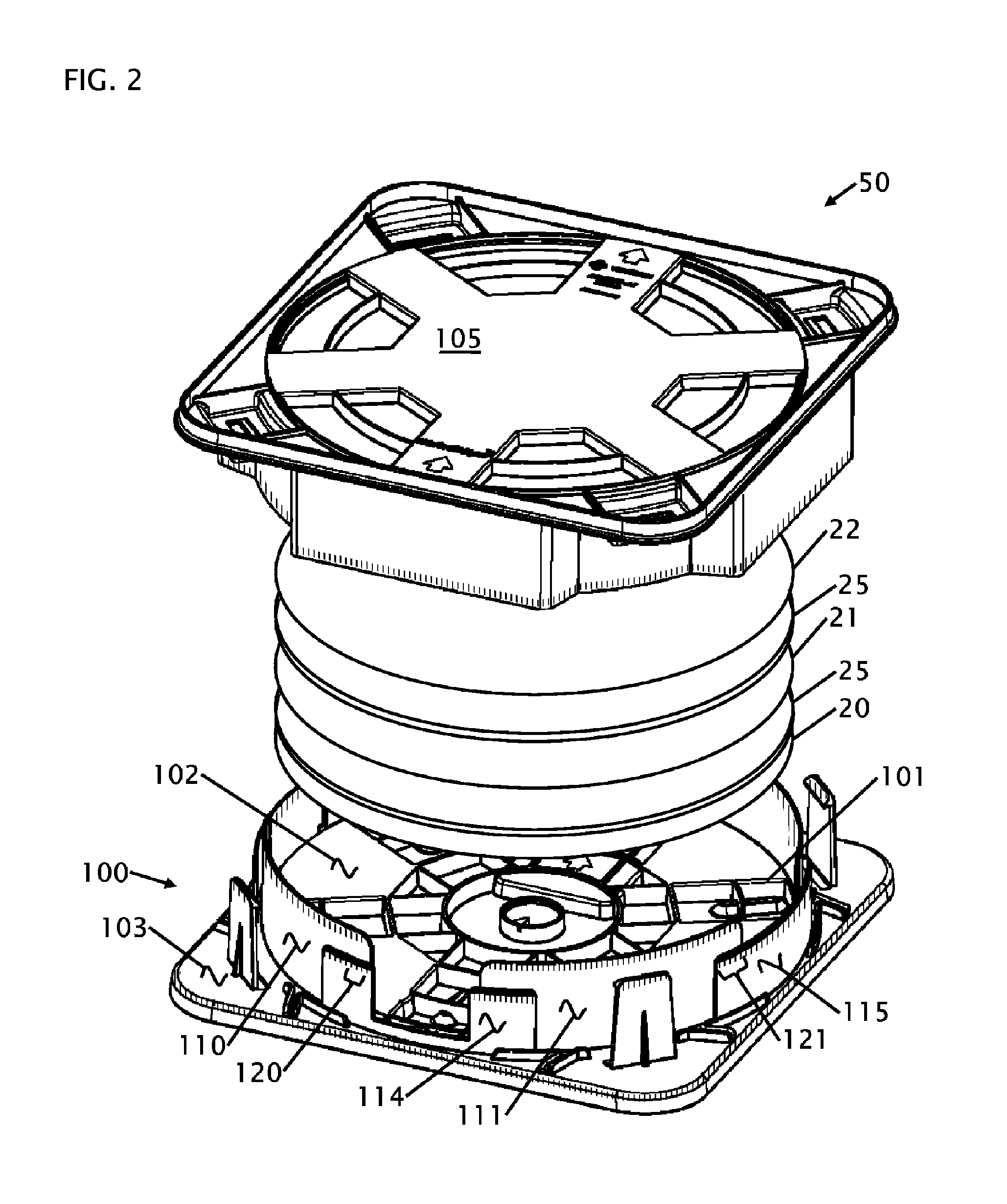
[0059]FIG. 1 and FIG. 2 show a perspective exploded view of the wafer container with a plurality of wafers disposed between the two wafer container clam shells. A plurality of semiconductor wafers 20, 21 and 22 are shown between the top 50 and bottom 100 housing with wafer separators or spacer rings 25. The top housing 50 has a planar top surface 105. The inside base surface 102 extends to the outside of the base surface 103 where the bottom housing has a ribbed pattern 101 that supports the bottom of the bottom most semiconductor wafer 20 and provides increased structural strength to the fairly plainer base surface 102 and 103. Both the top 50 and the bottom housings 100 have essentially planar rectangular or square bases. A plurality of inner rib walls 110 and 111that extend essentially perpendicular from the bottom housing 100 protect the semiconductor wafers 20-22 from shifting side damage. A rib 115 rises from the outer edge of the bottom housing to provide an area for labeling...


PUM


Abstract

Improvements in a semiconductor wafer container for reducing movement of semiconductor wafers within a wafer carrier using flexible wall segments, panels or flexible inserts in the base member's main inner containment diameter. These walls allow a vertical containment surface to move and capture the entire stack of wafers rather than a few wafers. The surface that contacts the wafers moves uniformly inward. The wafer stack is secured by reducing or eliminating the gap between the wafer container and the wafer stack. Further improvements include the addition of a ramped engagement surfaces in the top and/or bottom cover that provides mechanical advantage for easier assembly of the top and bottom cover. This design also allows for automated loading and unloading of the wafer stack because once the top cover is removed, the flexible walls spring back outward. Thus providing a small gap in which to freely remove the wafers.

Description

RELATED APPLICATIONS[0001]The present application is 1) a continuation-in-part of Ser. No. 12 / 749,448, filed on Mar. 29, 2010, now U.S. Pat. No. 8,556,079, issued Oct. 15, 2013; and 2) a continuation-in-part of Ser. No. 12 / 606,921, filed on Oct. 27, 2009; both of are continuations-in-part applications of Ser. No. 12 / 548,368, filed on Aug. 26, 2009, now U.S. Pat. No. 8,109,390, issued Feb. 7, 2012. The entire disclosure of all of the above applications is incorporated by reference herein, including all the drawings.FIELD OF THE INVENTION[0002]This invention relates to improvements in a container for the transportation of semiconductor wafers. More particularly, the present wafer container includes improvements in clamping sidewalls that prevent movement to the wafers, improved cover design to minimize rotation, a simplified top cover orientation mechanism and an improved bottom holding mechanism for automation.BACKGROUND OF THE DISCLOSURE[0003]In the processing of semiconductor wafer...

Claims


Application Information

Patent Timeline
Patent Type & Authority Applications(United States)
IPC IPC(8): H01L21/673
CPCH01L21/67373H01L21/67353H01L21/67369H01L21/67386
Inventor PYLANT, JAMES D.WABER, ALAN L.MACK, CHRISTOPHER R.
Owner TEXCHEM ADVANCED PRODS
Why Eureka
Try Eureka