Defect Injection For Transistor-Level Fault Simulation

a fault simulation and defect injection technology, applied in the field of integrated circuit (ic) testing technology, can solve the problems of two defects per element, more likely defects, and manufacturing process being more susceptible to short circuits between adjacent nodes than to open circuits

Active Publication Date: 2014-02-27
SIEMENS PROD LIFECYCLE MANAGEMENT SOFTWARE INC
View PDF2 Cites 18 Cited by
  • Summary
  • Abstract
  • Description
  • Claims
  • Application Information

AI Technical Summary

Problems solved by technology

Some defects are more likely than others; for example, a manufacturing process might be more susceptible to short circuits between adjacent nodes than to open circuits in connectors.
The step also includes injecting, one at a time, an open circuit in each resistor, capacitor, and inductor, and then a short circuit across each of them, resulting in two defects per element.
A shortcoming of this method is that the proximity of each circuit element in the layout is ignored, so circuit nodes that are adjacent to one another in the layout, hence more likely to have a short circuit defect between them, might not be simulated with this short circuit defect injected.
For many circuits, especially those including MOS transistors, a transistor-level simulator cannot simulate it if a portion of the circuit is entirely isolated from the rest of the circuit by the open circuit because the voltage between them becomes undefined.
Such a resistor, however, will have no effect on the DC voltage of the gate in a simulation if the resistor is connected between the gate and a DC voltage.
Also, such a resistor is not very realistic since a truly open-circuit in a connection to a transistor gate would likely result in the gate being charged to a high or low voltage during the IC manufacturing process.
Disadvantages of this method are that there are an infinite number of parameter variation combinations possible.
Simulating all possible shorts is generally impractical and pointless—for 100 nodes there are 100×99 / 2=4950 possible two-node connections, many of which might be impossible.
Fault simulation time is a key obstacle to practical analog fault simulation of industrial circuits.
The layout-extracted netlist of such a circuit may contain tens of thousands of parasitic capacitances and resistances, and hence potential defects.
Relaxing the accuracy of a simulation may reduce simulation time but could make it difficult to distinguish a test that fails due to simulation inaccuracy from a test that fails due to detecting an injected defect.
Simulating a random sample of defects may not simulate some of the most likely defects.
Using the design-intent netlist of a circuit for fault injection may mean that some of the most likely defects are not injected for simulation: shorts between adjacent conductors, and opens in long, narrow conductors.

Method used


Image

  • Defect Injection For Transistor-Level Fault Simulation
  • Defect Injection For Transistor-Level Fault Simulation
  • Defect Injection For Transistor-Level Fault Simulation

Examples


Embodiment Construction

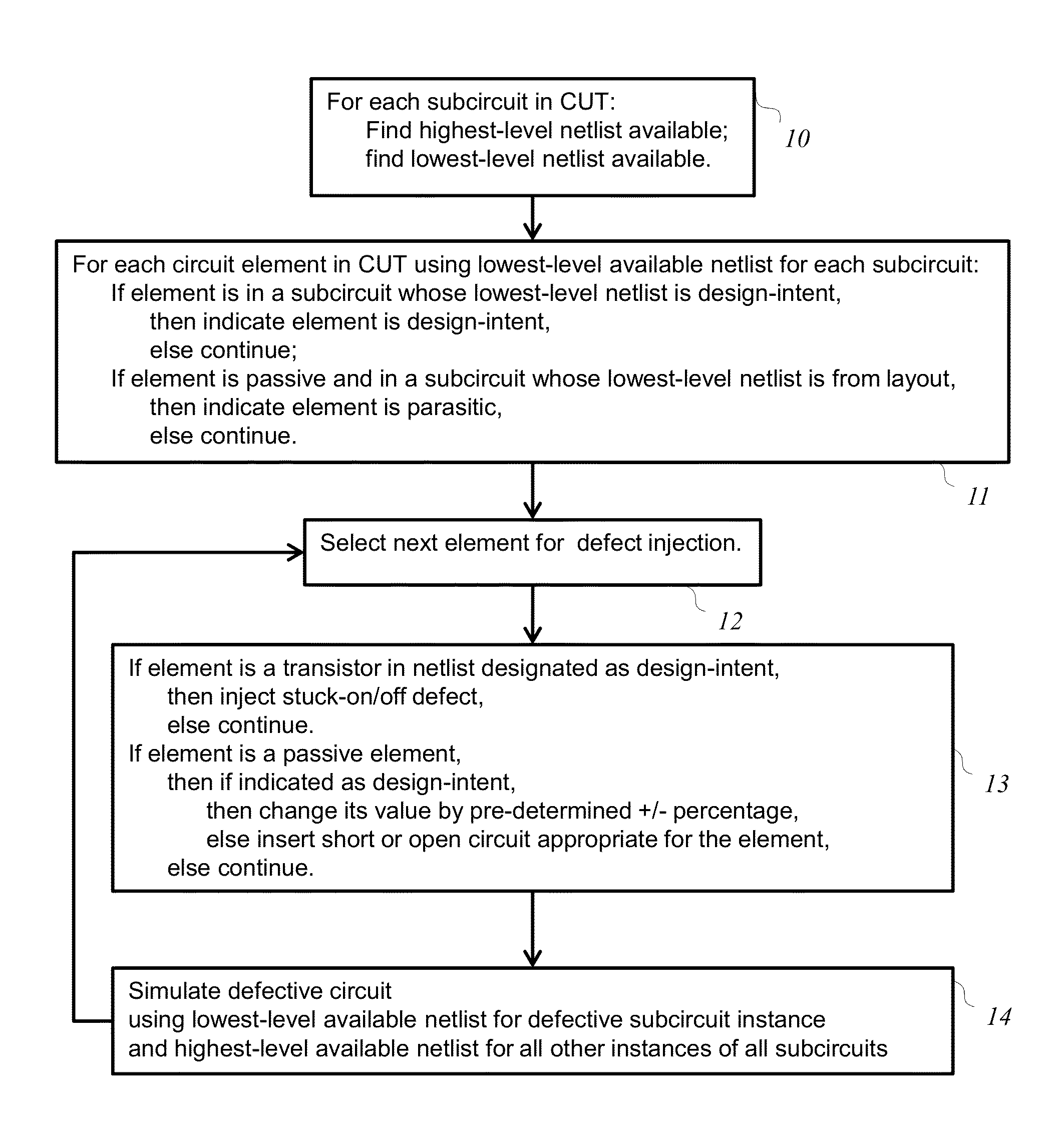
[0039]Various aspects of the present invention relate to techniques of defect injection for transistor-level fault simulation. In the following description, numerous details are set forth for the purpose of explanation. However, one of ordinary skill in the art will realize that the invention may be practiced without the use of these specific details. In other instances, well-known features have not been described in details to avoid obscuring the present invention.

[0040]Some of the techniques described herein can be implemented in software instructions stored on a computer-readable medium, software instructions executed on a computer, or some combination of both. Some of the disclosed techniques, for example, can be implemented as part of an electronic design automation (EDA) tool. Such methods can be executed on a single computer or on networked computers.

[0041]Although the operations of the disclosed methods are described in a particular sequential order for convenient presentati...


PUM


Abstract

Aspects of the invention relate to techniques of defect injection for transistor-level fault simulation. A circuit element in a circuit netlist of a circuit is first selected for defect injection. Next, a defect is determined based on whether the selected circuit element is a design-intent circuit element or a parasitic circuit element. After the defect is determined, the defect is injected into the circuit netlist and then the circuit is simulated.

Description

RELATED APPLICATIONS[0001]This application claims priority to U.S. Provisional Patent Application No. 61 / 691,939, entitled “A program and method for reducing the time to simulate possible defects in a circuit,” filed on Aug. 22, 2012, and naming Stephen Kenneth Sunter as inventor, which application is incorporated entirely herein by reference.FIELD OF THE INVENTION[0002]The present invention relates to the field of integrated circuit (IC) testing technology. Various implementations of the invention may be particularly useful for injecting possible defects into transistor-level netlists for fault simulation.BACKGROUND OF THE INVENTION[0003]Fault simulation measures or estimates the percentage of potential defects in a circuit that could be detected by a test applied to the circuit, by simulating the test applied to the circuit. A test comprises applying a set of stimuli (e.g., sine waves or digital patterns) to a circuit (e.g., an amplifier or logic gates), measuring parameters of th...

Claims


Application Information

Patent Timeline
Patent Type & Authority Applications(United States)
IPC IPC(8): G06F17/50
CPCG06F17/5009G06F30/367G06F30/33G06F30/20G06F30/3308
Inventor SUNTER, STEPHEN KENNETH
Owner SIEMENS PROD LIFECYCLE MANAGEMENT SOFTWARE INC
Why Eureka
Try Eureka