Eureka AIR delivers breakthrough ideas for toughest innovation challenges, trusted by R&D personnel around the world.

Parameter checking method for on-chip ESD protection circuit physical design layout verification

a protection circuit and physical design technology, applied in computer aided design, program control, instruments, etc., can solve the problems of insufficient esd protection design verification and failure of esd devices, and achieve the effect of improving the computing time efficiency of esd device recognition

Active Publication Date: 2007-07-10
TRUSTCHIP TECH
View PDF17 Cites 53 Cited by
  • Summary
  • Abstract
  • Description
  • Claims
  • Application Information

AI Technical Summary

Benefits of technology

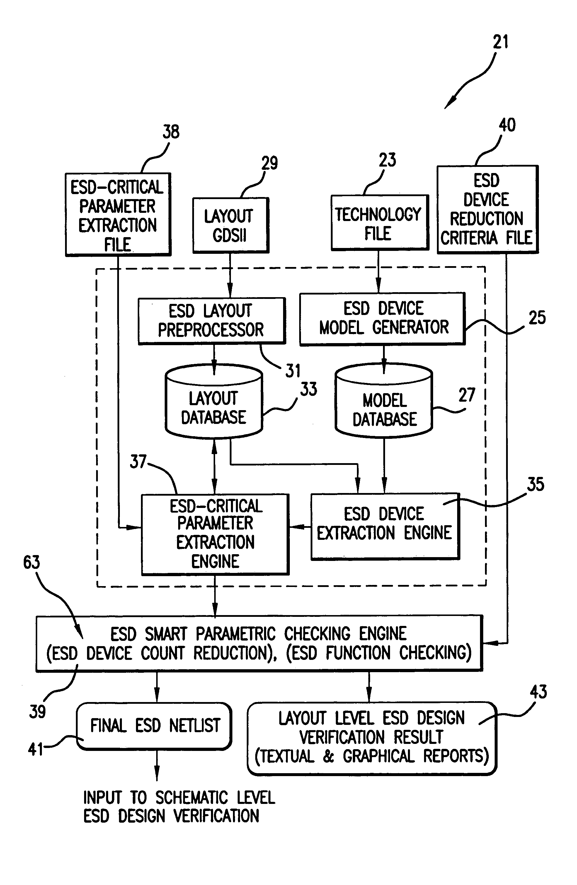
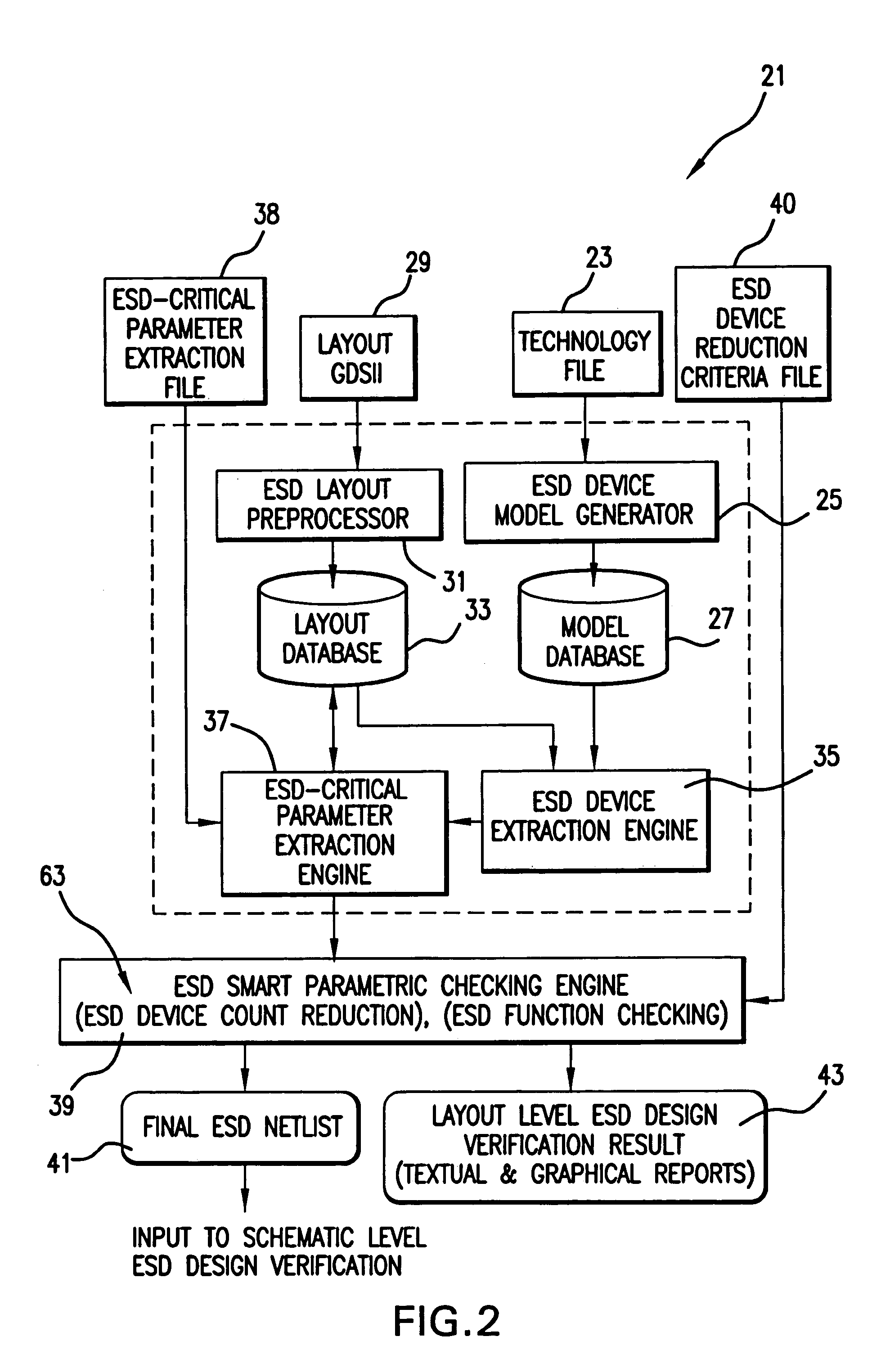
[0022]Generally, the present invention provides a new, smart, parameter checking mechanism that can perform complete ESD protection circuit design verification at the design layout level. One function of the smart parameter checking routine of the present invention is to ensure that all intentionally designed ESD devices are designed correctly in physical layout and that no potential parasitic ESD devices cause malfunction in ESD protection operation at full chip level.
[0024]By utilizing the ESD-critical parameters, the present invention can provide both extraction and analysis of the IC design layout for intentional and (unintentional) parasitic-type ESD devices. That is, after ESD device identification, the identified devices should be analyzed and the results compared to the IC requirements to verify the protection design validity for the whole chip.
[0029]Unlike a top-down approach, which handles each model graph individually, an algorithm according to the present invention may first explore the relationship between the device model graphs by a decomposition procedure. The common part of any two or more model graphs will only be matched for similarity once, which makes the device recognition procedure less heavily dependent upon the number of device model graphs than is the top-down approach. Further, according to certain aspects of the present invention, model containment relationships can be explicitly expressed, e.g., a small redundant ESD device contained in a larger ESD device can be easily removed from the final ESD device netlist. This eliminates the necessity of developing an individual redundant device processor and improves computing time efficiency for ESD device recognition.
[0030]The present invention can then perform a full chip level ESD protection physical design check. The present invention can determine if all the intentionally designed ESD devices exist in the extracted ESD protection circuit schematic. The present invention can extract the ESD-critical parameters of an ESD device based upon the approximate device physics equations for the specific ESD protection structures and given layout data. Then the present invention can perform a smart parameter checking routine which can verify the functionality of the intentionally designed ESD devices.

Problems solved by technology

Although simple DRC checking is needed to check spacings between IC masks for various diffusion layers, dielectric layers and metal interconnect layers, very similar to the routine for ordinary IC circuits, it is not enough for complete ESD protection design verification.
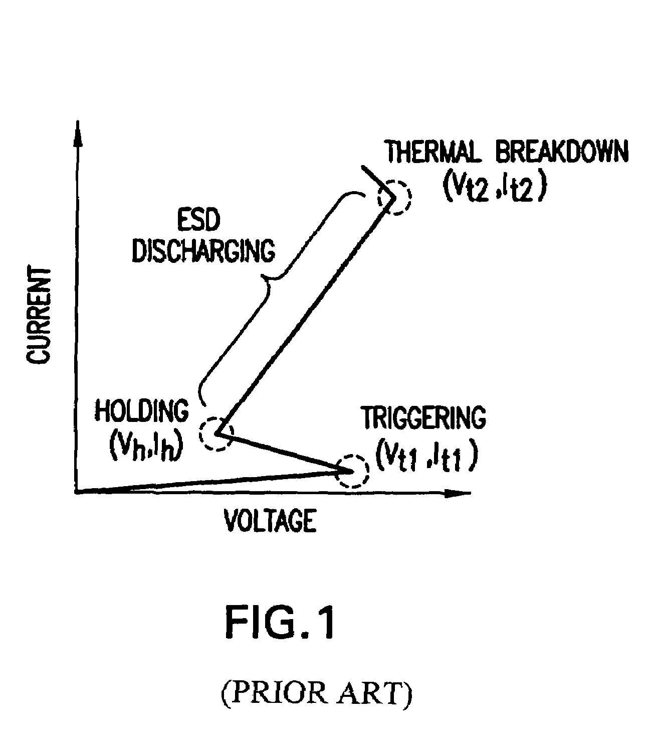
Eventually, the ESD device may fail as it reaches the second breakdown (thermal breakdown) point (Vt2, It2).

Method used


Image

  • Parameter checking method for on-chip ESD protection circuit physical design layout verification
  • Parameter checking method for on-chip ESD protection circuit physical design layout verification
  • Parameter checking method for on-chip ESD protection circuit physical design layout verification

Examples


example 1

[0131]As an example, a practical ESD protection circuit is used to demonstrate the function of the system. As shown in FIG. 8, the schematic with a core circuit (represented symbolically by an AND gate 71 and a CMOS output buffer 72) under protection, uses five types of ESD devices, i.e., a SCR ESD 73, a novel all-in-one ESD protection unit 75 at input, ggNMOS 74 and ggPMOS 76 paired ESD protection units at output, and a LVSCR 77 as power clamp protection unit. All ESD devices have been thoroughly tested in a commercial CMOS process.

[0132]As an example, a practical ESD protection circuit is used to demonstrate the function of the system. As shown in FIG. 8, the schematic with a core circuit (represented symbolically by an AND gate 71) under protection, uses three types of ESD devices, i.e., a SCR ESD 73, a novel all-in-one ESD protection unit 75 at input, ggNMOS and ggPMOS pair at output, and a LVSCR 77 as power clamp. All ESD devices have been thoroughly tested in a commercial CMOS...

example 2

[0155]As a second application example, the method of the present invention was applied to a specially designed IC chip with ESD protection circuitry shown in FIG. 11 where the core circuit 91 being protected is a symbolic digital gate and an output CMOS buffer 93. Five types of ESD protection structures are used including a LVSCR (low-V SCR) 94 at input-1, a Diode 95 at input-2, a complementary ggNMOS 97 and ggPMOS 99 (grounded-gate PMOS) pair at output pad 100 and a SCR 101 as the power clamp. This chip was designed and fabricated in a commercial 0.35 μm BiCMOS and tested for full function.

[0156]Auto extraction of all ESD-type devices and the corresponding ESD-critical parameters were conducted first with the initial complete ESD netlist generated, listed below, where each extracted ESD device is presented by its name, terminal nodes and ESD-critical parameters in a line.[0157]*complete netlist file created from D: / gdsii / demop6.gds[0158]LVSCR1 Input1 Gnd βNPNβPNP=62.62758 Vt1=8.861...


PUM


Abstract

A checking mechanism for complete full-chip ESD protection circuit design and layout verification at layout level identifies all of both intentional and parasitic ESD devices contained in the design layout file and compiles a netlist. The checking mechanism then determines the critical operating parameters of the identified ESD devices and determines if the parasitic devices will negatively effect ESD protection performance. The checking mechanism then determines if the intentional devices meet design specifications; eliminates parasitic devices which will not negatively effect ESD protection from the netlist, and retains those parasitic devices which may lead to ESD protection malfunction. Design layout verification and faults are then reported.

Description

BACKGROUND OF THE INVENTION[0001]Electrostatic discharge (ESD) induced damage is a devastating problem to integrated circuit (IC) parts. In order to protect IC parts against ESD failures, on-chip ESD protection circuits (hereinafter “ESD devices” for brevity) are required for virtually all practical IC products. On-chip ESD protection circuit design emerges as a major design challenge as IC technologies migrate into the very-deep-sub-micron (VDSM) regime, particularly for mixed-signal and RF ICs.[0002]ESD events, which are inevitable in IC manufacturing, assembly, and application, generate huge over-current and over-voltage transients that can fatally damage electronic components. ESD failure becomes a major IC reliability problem to the semiconductor industry, and accounts for 30–50% of total field failures. Therefore, on-chip ESD devices are required for all IC chips. In principle, an ESD protection device, which remains in the off state in normal operation, is triggered by an ESD...

Claims


Application Information

Patent Timeline
Patent Type & Authority Patents(United States)
IPC IPC(8): G06F17/50
CPCG06F17/5036G06F17/5081G06F30/367G06F30/398
Inventor WANG, ALBERT ZIHUIZHAN, ROUYING
Owner TRUSTCHIP TECH
Why Eureka
Eureka Blog
Learn More