

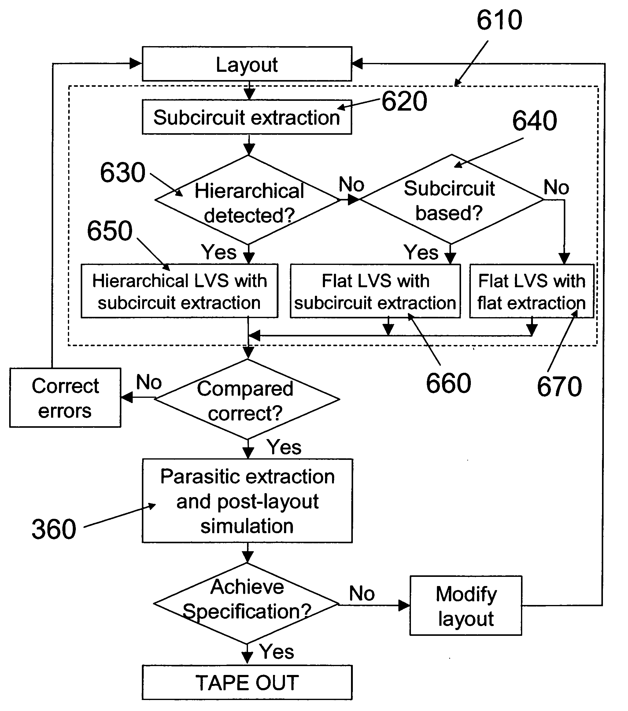
Method of checking the layout versus the schematic of multi-fingered MOS transistor layouts using a sub-circuit based extraction
a multi-fingered mos transistor and layout technology, applied in the field of very large-scale integrated circuit (vlsi) chip design, can solve the problems of inability to achieve a conventional flat extraction method, the performance of the circuit being manufactured may deviate significantly from the design target specifications, and the matching of two electrically equivalent child cells may be inappropria
- Summary
- Abstract
- Description
- Claims
- Application Information
AI Technical Summary
Benefits of technology
Problems solved by technology
Method used
Image

Examples
Embodiment Construction
[0043] The invention will now be described first by way of extracting all the geometric parameters of a MOS transistor layout to be followed by a description of performing the sub-circuit based layout versus schematic comparison.
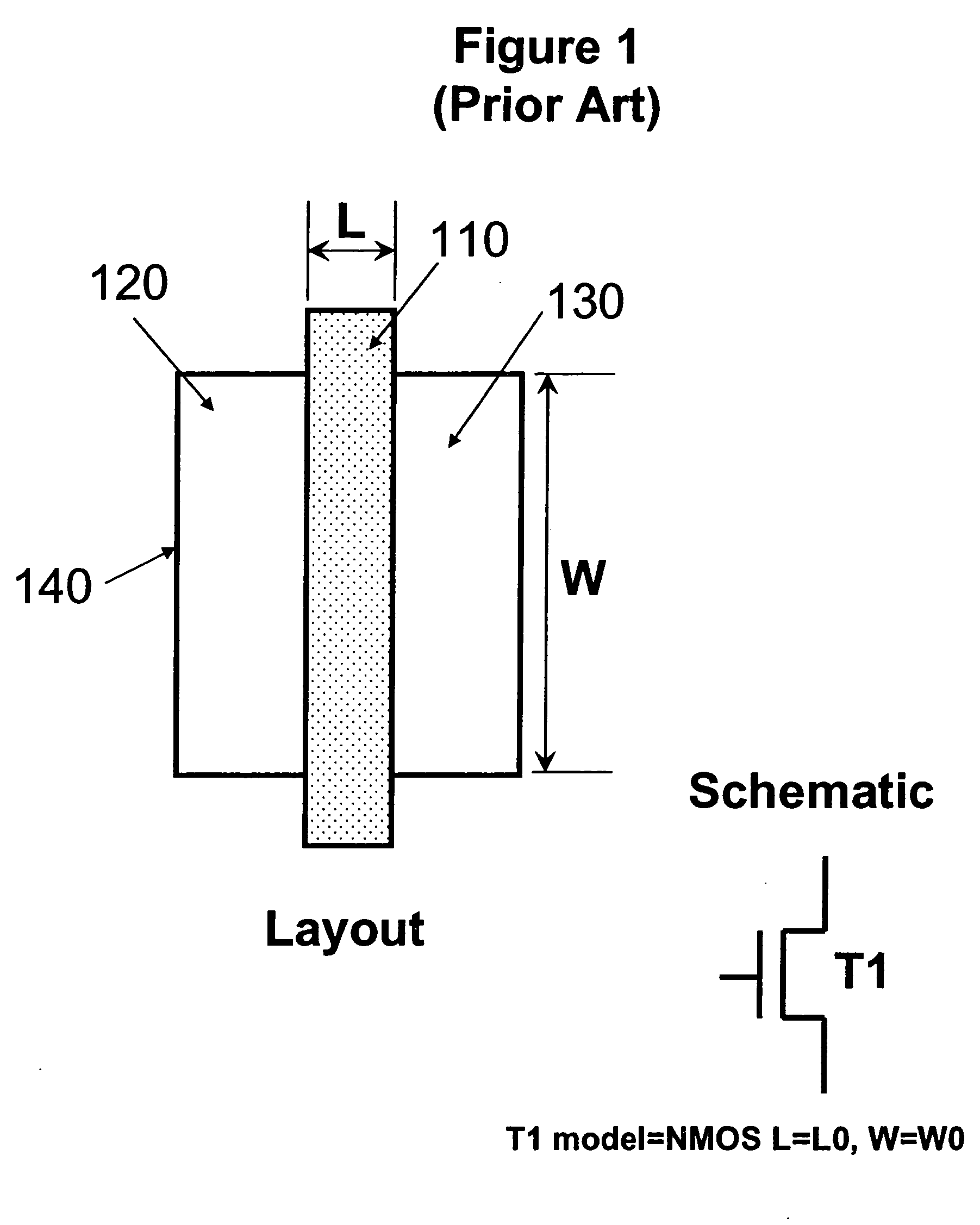
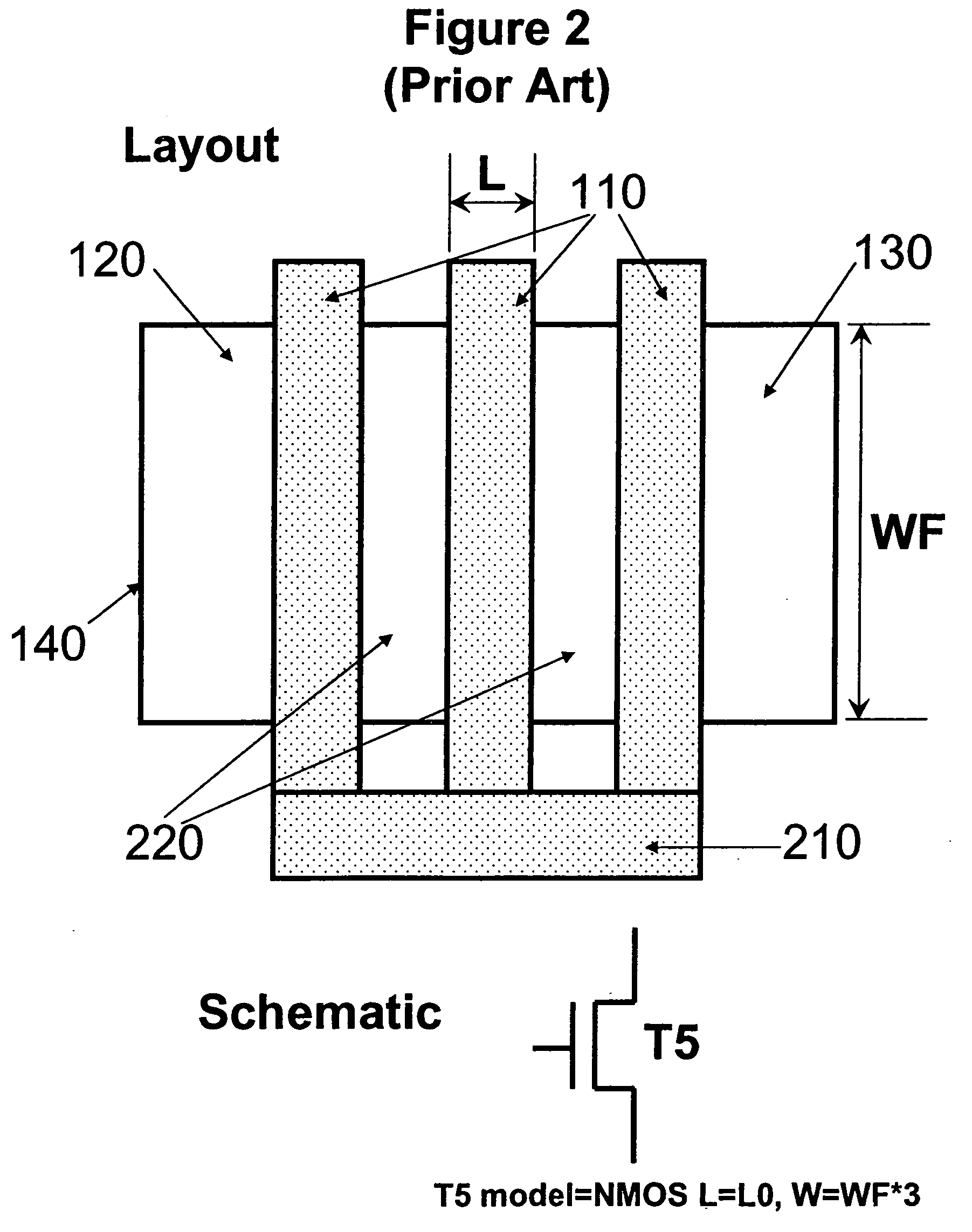
[0044] The main thrust of the invention is to extract the multi-fingered MOS transistor as one sub-circuit entity with all the geometric parameters such as the channel length and width, number of fingers, source and drain diffusion dimensions, and appropriate node connections included in the extracted netlist. To illustrate the inner workings of the invention, a parameterized sub-circuit MOS transistor with multi-finger layout is shown in FIG. 4. The geometric parameters are channel length “L”, channel width per finger “WF”, number of fingers “NF” (number count of 110s), left-side diffusion dimension “DIFFL”, right-side diffusion dimension “DIFFR”, and middle diffusion dimension “DIFFM”. The parameters “L”, “WF”, and “NF” are the same as those of a flat MOS...
PUM
 Abstract
Description
Claims
Application Information