Device having multiple printing layers and a printing method thereof
- Summary
- Abstract
- Description
- Claims
- Application Information
AI Technical Summary
Benefits of technology
Problems solved by technology
Method used
Image
Examples
Embodiment Construction
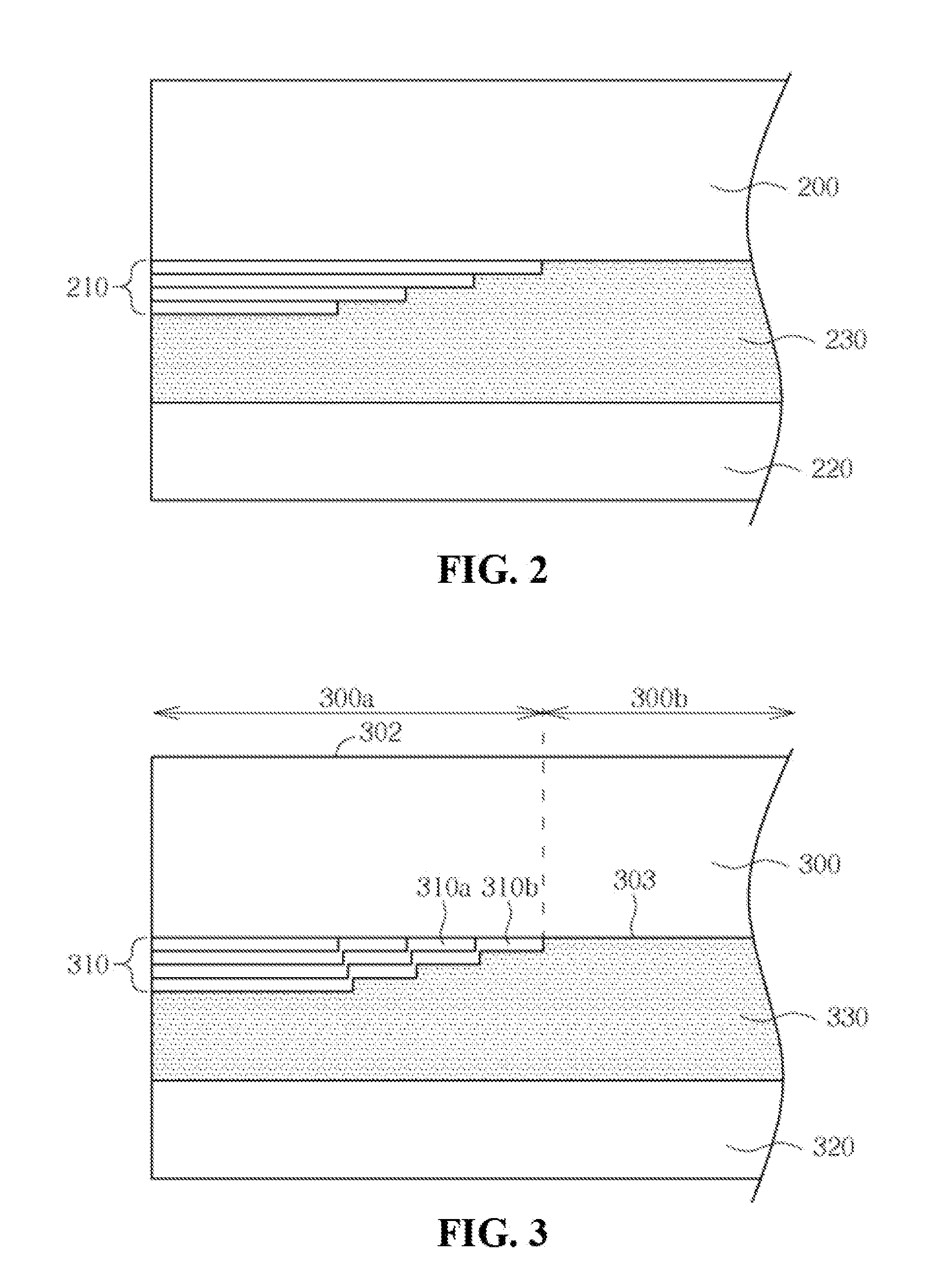
[0023]FIG. 3 illustrates a section view diagram of a device having multiple printing layers in accordance with embodiments of the present disclosure. FIG. 3 shows a state of a protective substrate 300 being laminated on a plate 320 (for example, an upper polarizer) in a display panel.
[0024]In this embodiment, the protective substrate 300 is provided as a protective layer for protecting said plate 320 underneath, such as a touch substrate having a touch sensing layer or an upper polarizer of display panel. Material of the protective substrate 300 can be a transparent glass such as a cover glass or plastic. As shown in FIG. 3, the protective substrate 300 can be divided into a peripheral area 300a and a non-peripheral area 300b, which is surrounded by the peripheral area 300a. The peripheral area 300a can be a pattern area, which is printed with an opaque ink pattern for defining border of the device or endowing the device with changes of colors for design. The non-peripheral area 300...
PUM
| Property | Measurement | Unit |
|---|---|---|
| Size | aaaaa | aaaaa |
| Area | aaaaa | aaaaa |
Abstract
Description
Claims
Application Information


