Liquid crystal display device

a display device and liquid crystal technology, applied in the direction of instruments, static indicating devices, etc., can solve the problems of increasing directly affecting the length of continuous operation time, and reducing the power consumption of the display device, so as to reduce power consumption, improve image quality, and improve the effect of definition

Inactive Publication Date: 2014-04-17
SEMICON ENERGY LAB CO LTD
View PDF15 Cites 14 Cited by
  • Summary
  • Abstract
  • Description
  • Claims
  • Application Information

AI Technical Summary

Benefits of technology

[0010]Recently, reducing the power consumption of electronic devices has been required for energy saving, and reducing the power consumption of liquid crystal display devices has also been required. In particular, further reducing power consumption is needed for portable electronic devices such as mobile phones, mobile phones with advanced features (smartphones), tablet terminals, and notebook PCs because reducing the power consumption of their display devices directly affects the length of continuous operating time.
[0011]Further, in the case of such a portable electronic device, the distance between the liquid crystal display device and the user's eyes is short; thus, increasing the definition of the liquid crystal display device is needed. Further, increasing the definition is needed also for a large-sized liquid crystal display device such as a TV in order to have image quality better than full high-definition image quality.
[0012]When the definition of a liquid crystal display device is increased for these reasons, the area of each pixel is inevitably reduced, and the areas of a transistor and a capacitor to a pixel are increased. Accordingly, in a transmissive liquid crystal display device, a region of a pixel through which light emitted from a backlight transmits is reduced, so that the aperture ratio is decreased. When the aperture ratio is decreased, the light of the backlight has to be stronger in order to compensate the luminance. Accordingly, the power consumption of the backlight is increased, so that the power consumption of the liquid crystal display device is also increased.

Problems solved by technology

In particular, further reducing power consumption is needed for portable electronic devices such as mobile phones, mobile phones with advanced features (smartphones), tablet terminals, and notebook PCs because reducing the power consumption of their display devices directly affects the length of continuous operating time.
Further, in the case of such a portable electronic device, the distance between the liquid crystal display device and the user's eyes is short; thus, increasing the definition of the liquid crystal display device is needed.
Accordingly, the power consumption of the backlight is increased, so that the power consumption of the liquid crystal display device is also increased.
Thus, the period during which the potential of a pixel electrode can be held becomes shorter, so that a problem of a reduction in image quality occurs.

Method used


Image

  • Liquid crystal display device
  • Liquid crystal display device
  • Liquid crystal display device

Examples


modification example 1

of Structure of Pixel

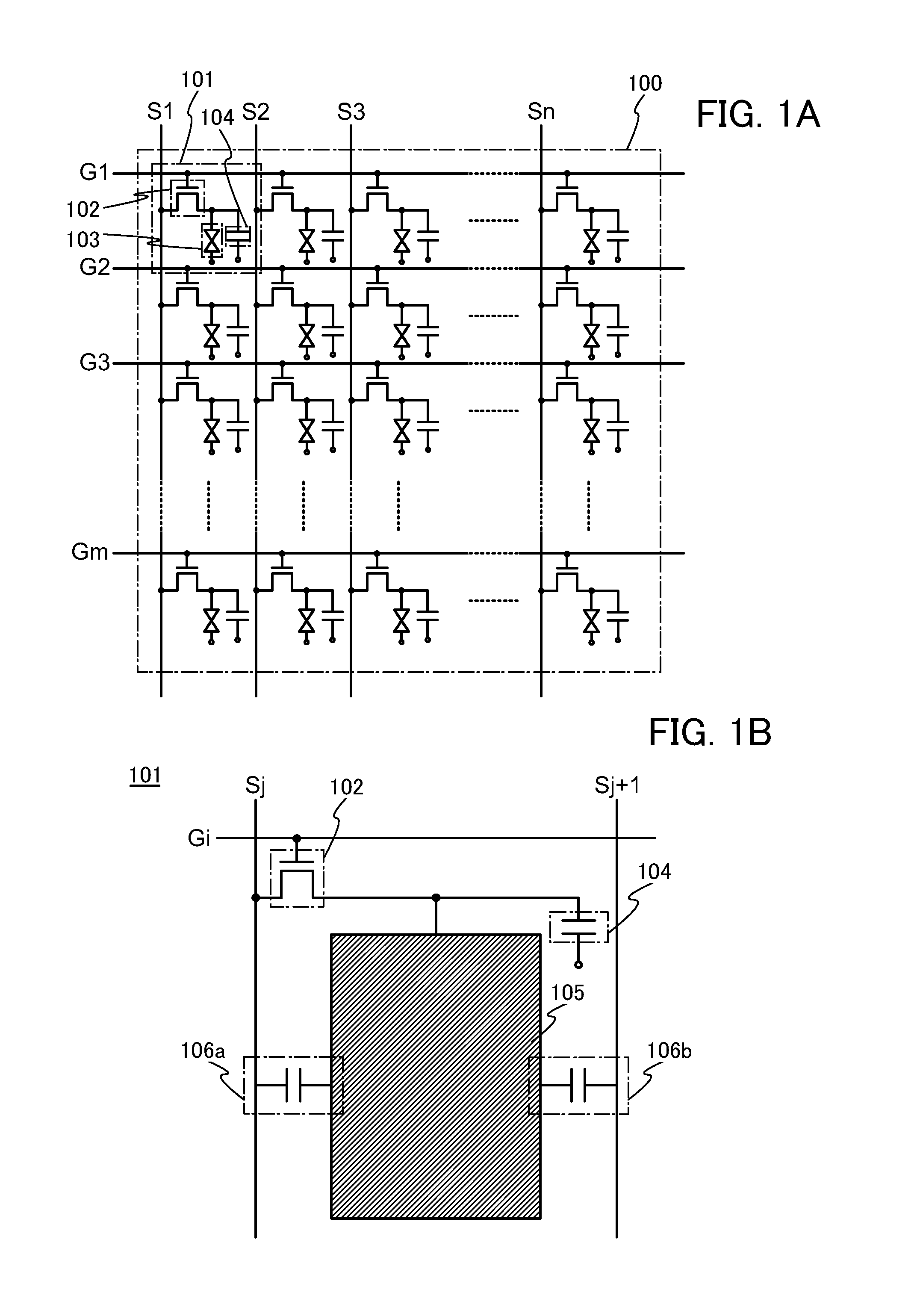
[0176]As the liquid crystal display device of one embodiment of the present invention, a structure where the capacitor line 204 is provided to form the capacitor 104 is illustrated in FIG. 7; however, the present invention is not limited thereto. In the case where sufficient capacitance can be formed in the pixel electrode even if a capacitor line is not provided intentionally, the liquid crystal display device may have a structure of the pixel in which a capacitor line is not provided in FIG. 11. At this time, a capacitor including a capacitor line does not exist; thus, the capacitance value of the capacitor is 0 fF in an equivalent circuit diagram. The structure of the pixel of the liquid crystal display device in FIG. 11 is the same as that of the pixel of the liquid crystal display device in FIG. 7 except that the capacitor line is not provided; thus, the description of FIG. 7 or the like can be referred to for the details.

modification example 2

of Structure of Pixel

[0177]The liquid crystal display device of one embodiment of the present invention in FIG. 7 is assumed to have a stripe arrangement in which a plurality of pixels are provided in a matrix; however, the present invention is not limited thereto. For example, as illustrated in FIG. 12A, a structure in which a plurality of pixels is provided in a delta arrangement can also be used. In the pixel structures in FIG. 7 and FIG. 11, the source lines are provided in a straight line and extend in the row direction. In the case where the pixels are provided in a delta arrangement as illustrated in FIG. 12A, the source lines are provided to each have an S-shaped curve in accordance with the delta arrangement of a pixel 111 and extend in the column direction. The pixel structure illustrated in FIG. 12A is the same as that of the liquid crystal display device in FIG. 11 except that the source lines are provided to each have an S-shaped curve and extend in the column direction...


PUM


Abstract

A liquid crystal display device which has higher definition and reduced power consumption while its image quality is maintained is provided. A switching transistor of an active matrix liquid crystal display device is formed using a transistor having an extremely low off-state current to reduce the area of a capacitor; the capacitance value of parasitic capacitance formed by the left end of a pixel electrode and a first source line is made to be approximately the same as that of parasitic capacitance formed by the right end of the pixel electrode and a second source line; and video signals having one polarity are input to the first source line, and video signals having the other polarity are input to the second source line.

Description

BACKGROUND OF THE INVENTION[0001]1. Field of the Invention[0002]The present invention relates to a liquid crystal display device, particularly an active matrix liquid crystal display device having a transistor including an oxide semiconductor.[0003]2. Description of the Related Art[0004]Recently, a metal oxide called an oxide semiconductor has attracted attention as an active layer of a new semiconductor element instead of amorphous silicon or polysilicon. An oxide semiconductor exhibits both high mobility which is a feature of polysilicon and microcrystalline silicon and uniform element characteristics, which are a feature of amorphous silicon.[0005]Examples of such an oxide semiconductor are tungsten oxide, tin oxide, indium oxide, and zinc oxide. In particular, an In—Ga—Zn-based oxide semiconductor which is a metal oxide including indium, gallium, and zinc brings about excellent transistor characteristics, and thus has attracted attention as an active layer of a next-generation t...

Claims


Application Information

Patent Timeline
Patent Type & Authority Applications(United States)
IPC IPC(8): G09G3/36
CPCG09G3/3614G09G3/3659G09G2300/0852G09G2320/0214
Inventor YAMAZAKI, SHUNPEIMIYAKE, HIROYUKI
Owner SEMICON ENERGY LAB CO LTD
Why Eureka
Try Eureka