Pressed-contact type semiconductor device and method for manufacturing the same

a semiconductor element and contact technology, applied in semiconductor devices, semiconductor/solid-state device details, electrical devices, etc., can solve the problems of difficult to realize a surface contact between the electrode of the semiconductor element and the lead frame (electrode) with uniform pressure, and the connection resistance value is not stabilized, so as to achieve stable connection resistance value

Active Publication Date: 2014-04-24
PANASONIC INTELLECTUAL PROPERTY MANAGEMENT CO LTD
View PDF2 Cites 10 Cited by
  • Summary
  • Abstract
  • Description
  • Claims
  • Application Information

AI Technical Summary

Benefits of technology

[0047]The present invention can provide a semiconductor device and a method for manufacturing the same, which can absorb the dimensional variation of the various components, which constitute the press

Problems solved by technology

However, in a power semiconductor device of such a configuration, since a coefficient of linear expansion of the lead frame (electrode) and a coefficient of linear expansion of the power semiconductor element are greatly different, large heat stress is applied repeatedly to the solder joining part by a power cycle at the time of making the power semiconductor device drive, finally, a solder crack occurs and a problem of joining failure arises.
However, in the case of such a pressed-contact type power semiconductor device, it is difficult to realize a surface contac

Method used


Image

  • Pressed-contact type semiconductor device and method for manufacturing the same
  • Pressed-contact type semiconductor device and method for manufacturing the same
  • Pressed-contact type semiconductor device and method for manufacturing the same

Examples


embodiment

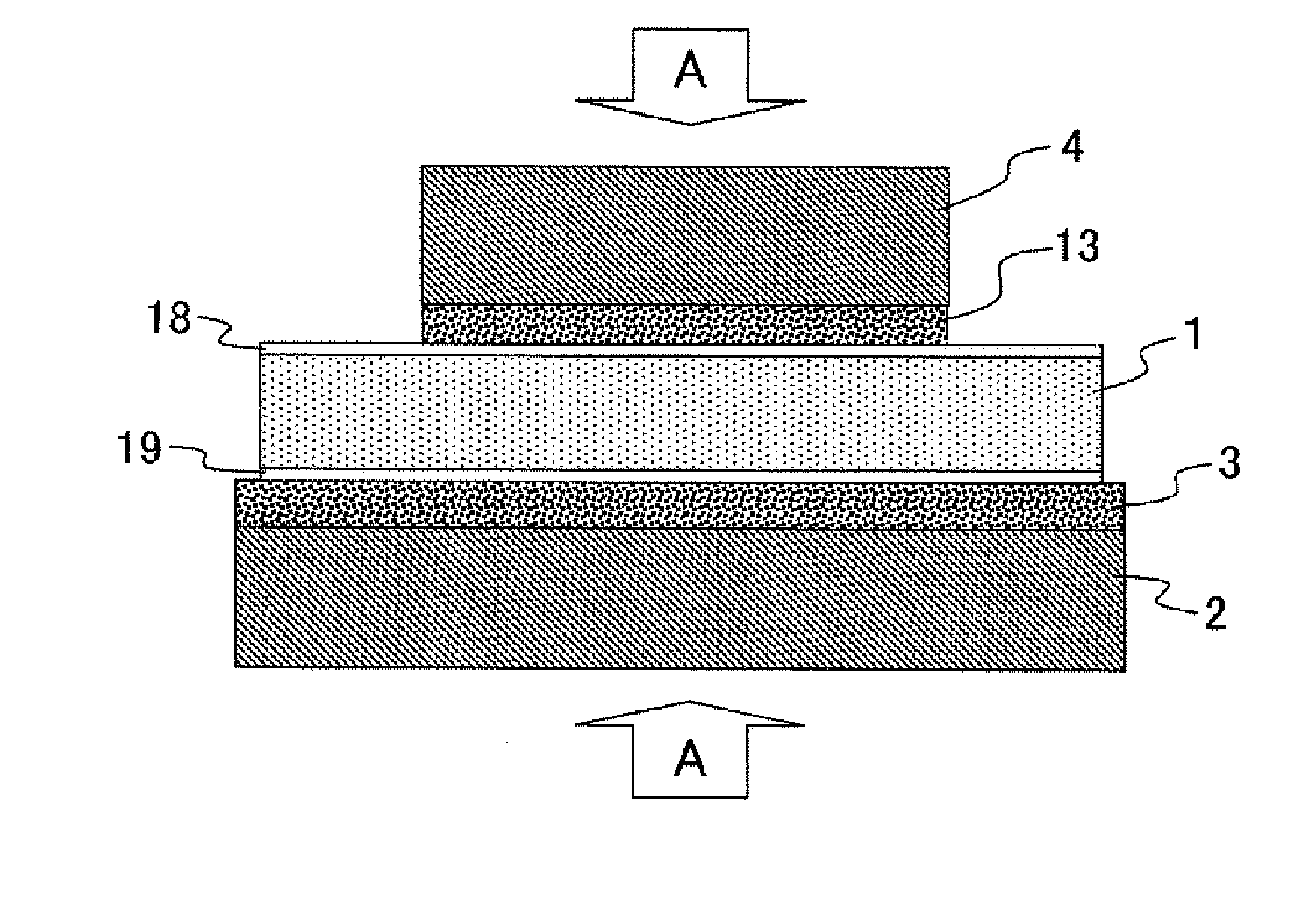
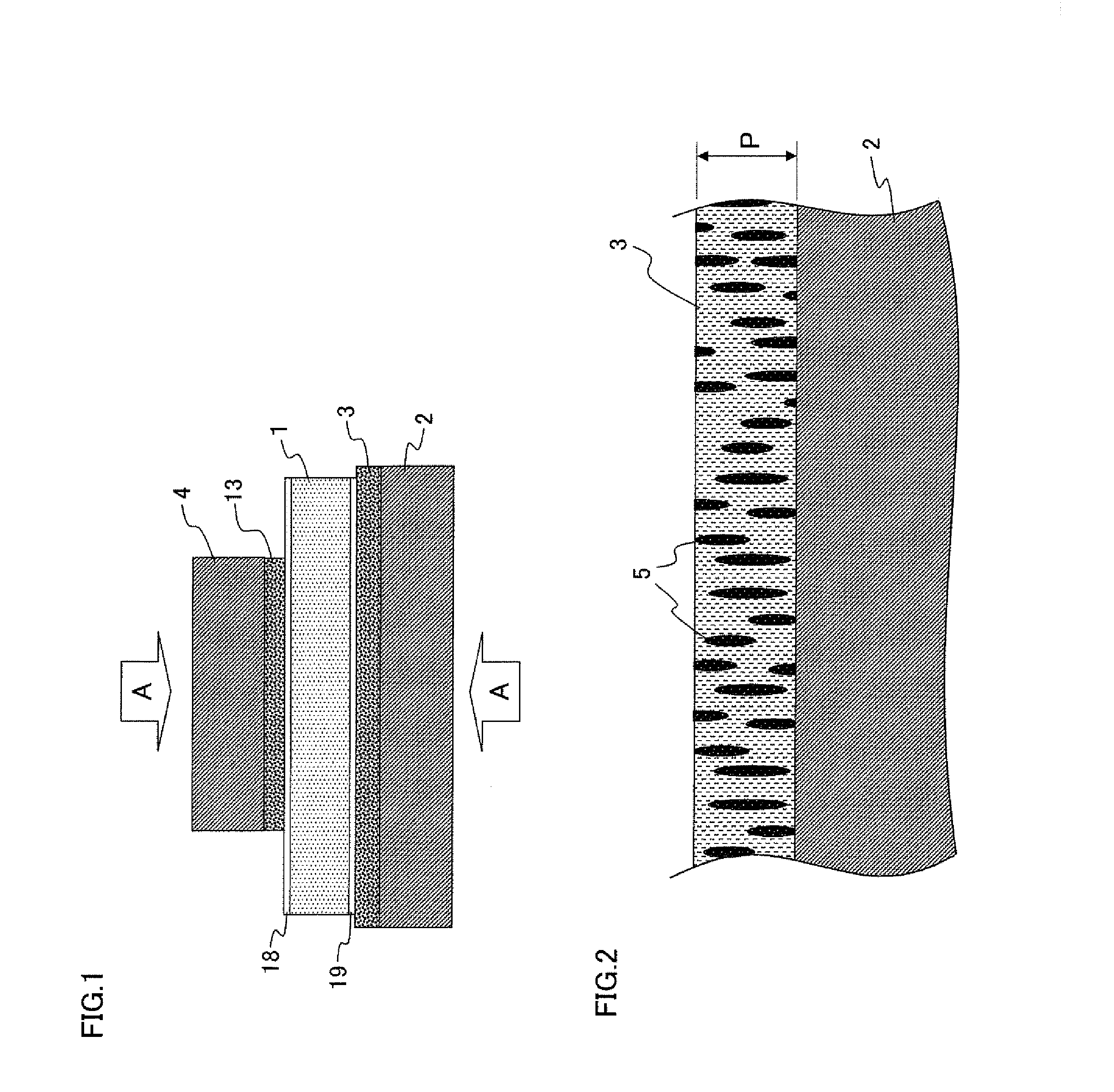
[0061]FIG. 1 is a schematic sectional view showing a configuration of the pressed-contact type power semiconductor device according to an embodiment of the present invention.

[0062]As shown in FIG. 1, a lead frame 4 with a metallic porous plating layer 13 formed on the lower surface thereof is disposed over an upper electrode 18 of a power semiconductor element 1, and a lead frame 2 with a metallic porous plating layer 3 formed on the upper surface thereof is disposed under a lower electrode 19 of the power semiconductor element 1. A pressed-contact joining is carried out by always applying an applied pressure A with the orientations facing each other with respect to the lead frame 2 and the lead frame 4. And then, the electrical continuity between the upper electrode 18 of the power semiconductor element 1 and the lead frame 4, and the electrical continuity between the lower electrode 19 of the power semiconductor element 1 and the lead frame 2 are obtained.

[0063]By the way, the upp...

example

[0097]Next, mainly referring to FIGS. 7(a), 7(b), and 8, a pressed-contact type power semiconductor device which is one example of the pressed-contact type semiconductor device of the present invention is described more concretely.

[0098]By the way, the components that are the same as those of the above described embodiment are denoted by the same reference numerals.

[0099]FIG. 7(a) is a schematic sectional view of a pressed-contact type power semiconductor device of the present example. The pressed-contact type power semiconductor device shown in FIG. 7(a) is one example of the configuration which is shown in FIG. 5(c) and described in the above embodiment.

[0100]FIG. 7(b) is a schematic sectional view of a pressed-contact type power semiconductor device as a comparative example in which the conventional soft metal sheet 103 is used. Since the pressed-contact type power semiconductor device shown in FIG. 7(b) fundamentally has the same configuration as the conventional pressed-contact...


PUM


Abstract

A pressed-contact type semiconductor device includes a power semiconductor element, on an upper surface of which at least a first electrode is formed and on a lower surface of which at least a second electrode is formed, lead frames which face the first electrode and the second electrode of the power semiconductor element respectively, and a clip which applies a pressure to the lead frames while the power semiconductor element is sandwiched by the lead frames, wherein a metallic porous plating part is formed on a surface which faces the first electrode or the second electrode, the surface being a surface of at least one of the lead frames.

Description

CROSS-REFERENCE TO RELATED APPLICATIONS[0001]This application is a U.S. national phase application of PCT International Patent Application No. PCT / JP2012 / 006712 filed Oct. 19, 2012, claiming the benefit of priority of Japanese Patent Application No. 2012-002878 filed Jan. 11, 2012, all of which are incorporated by reference herein in their entirety.TECHNICAL FIELD[0002]The present invention relates to a pressed-contact type semiconductor device and a method for manufacturing the same.BACKGROUND ART[0003]The power electronics technology which controls the main circuit current by using a power semiconductor element is applied in broad fields such as major appliances, a railroad and an electric vehicle.[0004]In late years, as the power semiconductor element, the element to which more efficient materials such as SiC (Silicon Carbide) or GaN (Gallium Nitride) are applied attracts attention in addition to the IGBT (Insulation Gate type Bipolar Transistor) and the MOSFET (Metal-Oxide-Semic...

Claims


Application Information

Patent Timeline
IPC IPC(8): H01L23/495H01L23/00
CPCH01L24/89H01L23/495H01L24/72H01L2924/13091H01L2924/13055H01L23/4093H01L23/49562H01L23/49582H01L2924/1306H01L24/90H01L2924/1305H01L2924/351H01L2924/00
Inventor TSUKAHARA, NORIHITOKOJIMA, TOSHIYUKIHIROSE, TAKAYUKIIKUTA, KEIKOTANDA, KOHICHI
Owner PANASONIC INTELLECTUAL PROPERTY MANAGEMENT CO LTD
Why Eureka
Try Eureka