Array Substrate and Method for Fabricating Array Substrate, and Display Device
- Summary
- Abstract
- Description
- Claims
- Application Information
AI Technical Summary
Benefits of technology
Problems solved by technology
Method used
Image

Examples
embodiment 1
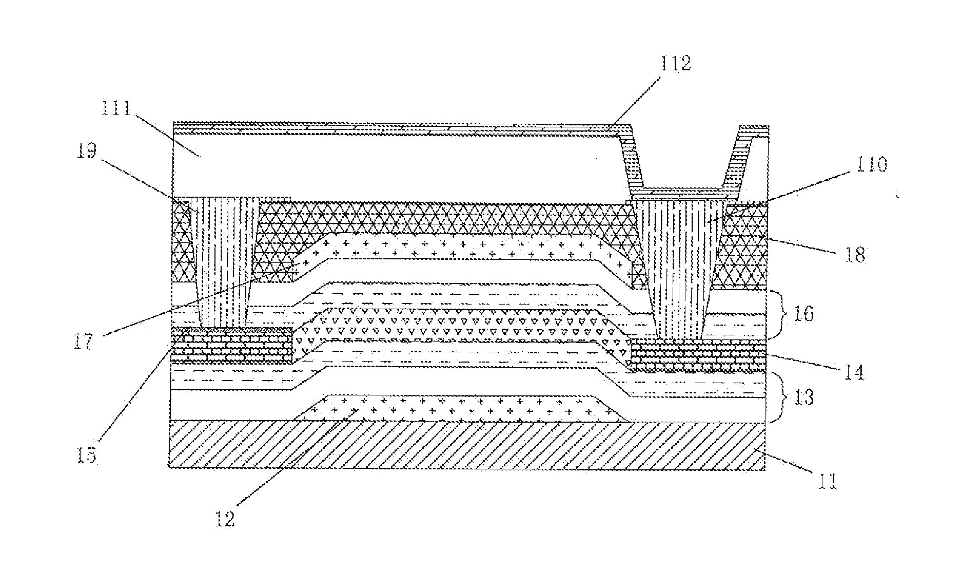
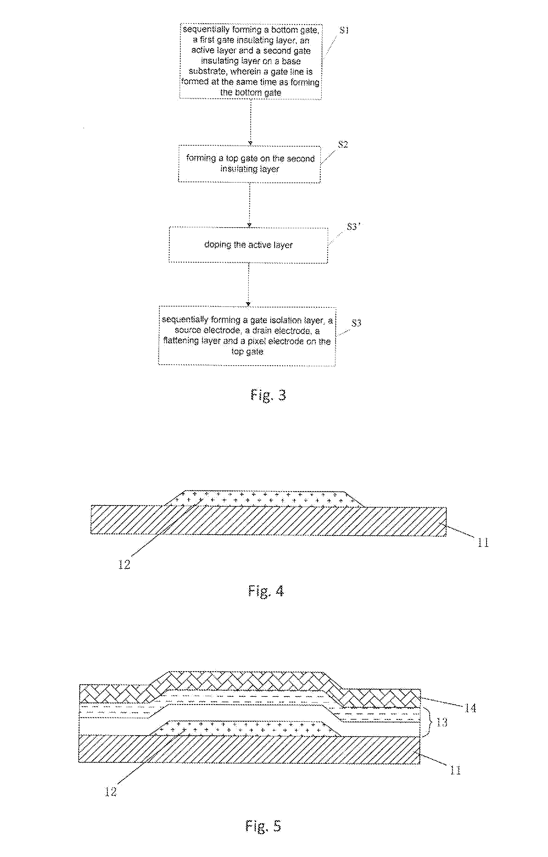
[0037]As illustrated in FIG. 1, the present invention provides an array substrate, which includes: a base substrate 11, a TFT, a gate line, a data line and a pixel electrode 112 formed on the base substrate 11, the TFT includes: a bottom gate 12, a first gate insulating layer 13, an active layer 14, a second gate insulating layer 16, a top gate 17, a gate isolation layer 18 and a source electrode 19 and a drain electrode 110 sequentially formed on the base substrate 11, wherein material of the gate isolation layer 18 includes SiO2 and / or SiNx.
[0038]In this embodiment, forming inversion layers at both upper and lower surfaces of a silicon film at the same time can be achieved in a situation where a proper silicon film is selected, carrier concentrations in the inversion layers of both upper and lower surfaces increase rapidly with the increase of gate voltage in a situation where the silicon film is fully depleted, and the driving ability and sub-threshold and frequency response char...
embodiment 2
[0044]As illustrated in FIG. 2, the array substrate of this embodiment has a structure substantially the same as that of the array substrate of Embodiment 1, and also includes: a base substrate 11, a TFT, a gate line, a data line and a pixel electrode 112 formed on the base substrate 11, the TFT includes: a bottom gate 12, a first gate insulating layer 13, an active layer 14, a second gate insulating layer 16, a top gate 17, a gate isolation layer 18 and a source electrode 19 and a drain electrode 110 sequentially formed on the base substrate 11, wherein the gate isolation layer 18 includes SiNx.
[0045]Wherein, the source electrode 19 and the drain electrode 110 are in contact with the active layer 14 through a first via hole 191 and a second via hole 1101 passing through the gate isolation layer 18 and the second insulating layer 16, respectively; the pixel electrode 112 is in contact with the drain electrode 110.
[0046]The array substrate further includes: a flattening layer 111 loc...
embodiment 3
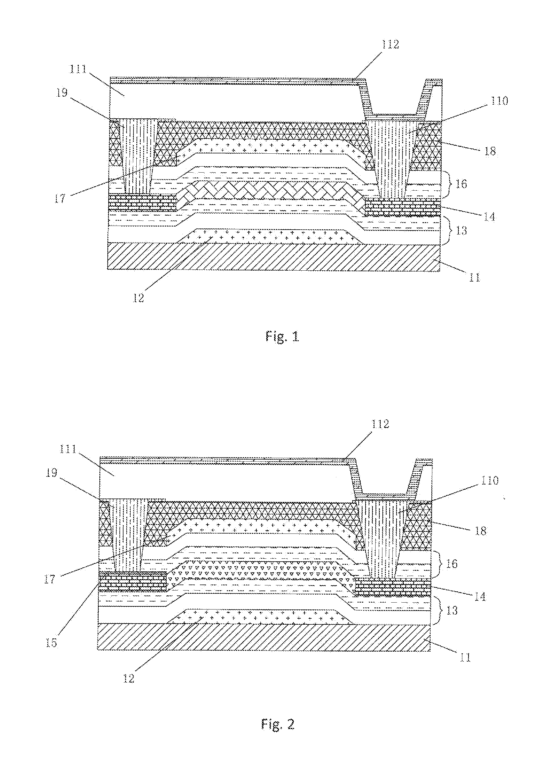
[0052]The array substrate of this embodiment has a structure substantially the same as those of the array substrates of Embodiment 1 and Embodiment 2, and also includes: a base substrate 11, a TFT, a gate line, a data line and a pixel electrode 112 formed on the base substrate 11, the TFT includes: a bottom gate 12, a first gate insulating layer 13, an active layer 14, a second gate insulating layer 16, a top gate 17, a gate isolation layer 18 and a source electrode 19 and a drain electrode 110 sequentially formed on the base substrate 11, wherein the gate isolation layer 16 includes SiO2.
[0053]Wherein, the source electrode 19 and the drain electrode 110 are in contact with the active layer 14 through a first via hole 191 and a second via hole 1101 passing through the gate isolation layer 18 and the second insulating layer 16, respectively; the pixel electrode 112 is in contact with the drain electrode 110.
[0054]The array substrate further includes: a flattening layer 111 located be...
PUM
 Abstract
Description
Claims
Application Information
 - R&D Engineer
- R&D Manager
- IP Professional
- Industry Leading Data Capabilities
- Powerful AI technology
- Patent DNA Extraction
Browse by: Latest US Patents, China's latest patents, Technical Efficacy Thesaurus, Application Domain, Technology Topic.
© 2024 PatSnap. All rights reserved.Legal|Privacy policy|Modern Slavery Act Transparency Statement|Sitemap