Supercharge Your Innovation With Domain-Expert AI Agents!

Use Disposable Gate Cap to Form Transistors, and Split Gate Charge Trapping Memory Cells

a technology of memory cells and gate caps, which is applied in the direction of basic electric elements, electrical apparatus, semiconductor devices, etc., can solve the problems of difficult integration of memory cells, such as split-gate memory cells, with the processing of one or more types of non-memory transistors on the same substra

Inactive Publication Date: 2014-06-19
CYPRESS SEMICON CORP
View PDF6 Cites 4 Cited by
  • Summary
  • Abstract
  • Description
  • Claims
  • Application Information

AI Technical Summary

Benefits of technology

The patent text describes a method and structure for fabricating semiconductor devices with transistors and memory cells. The method includes disposing a gate layer over a dielectric layer on a substrate and etching through the cap layer and the gate layer to define the transistor gates. The method also includes forming a plurality of memory cells in a first region of the substrate with a memory gate and a select gate, and a doped region in the substrate adjacent to the memory gate. The method further includes etching through the cap layer and the gate layer in a second region of the substrate to define the first transistor gate. The final thickness of the first transistor gate is substantially equal to the combined thickness of the cap layer and the gate layer. The technical effect of the patent text is to provide a method for fabricating semiconductor devices with improved transistor and memory cell density.

Problems solved by technology

High drain and gate voltages are used to facilitate the programming process, and the memory cell conducts relatively high current during programming, which can be undesirable in low voltage or low power applications.
Integrating the processing of memory cells, such as a split-gate memory cell, with the processing of one or more types of non-memory transistors on the same substrate is challenging as each requires different fabrication parameters.

Method used


Image

  • Use Disposable Gate Cap to Form Transistors, and Split Gate Charge Trapping Memory Cells
  • Use Disposable Gate Cap to Form Transistors, and Split Gate Charge Trapping Memory Cells
  • Use Disposable Gate Cap to Form Transistors, and Split Gate Charge Trapping Memory Cells

Examples


Embodiment Construction

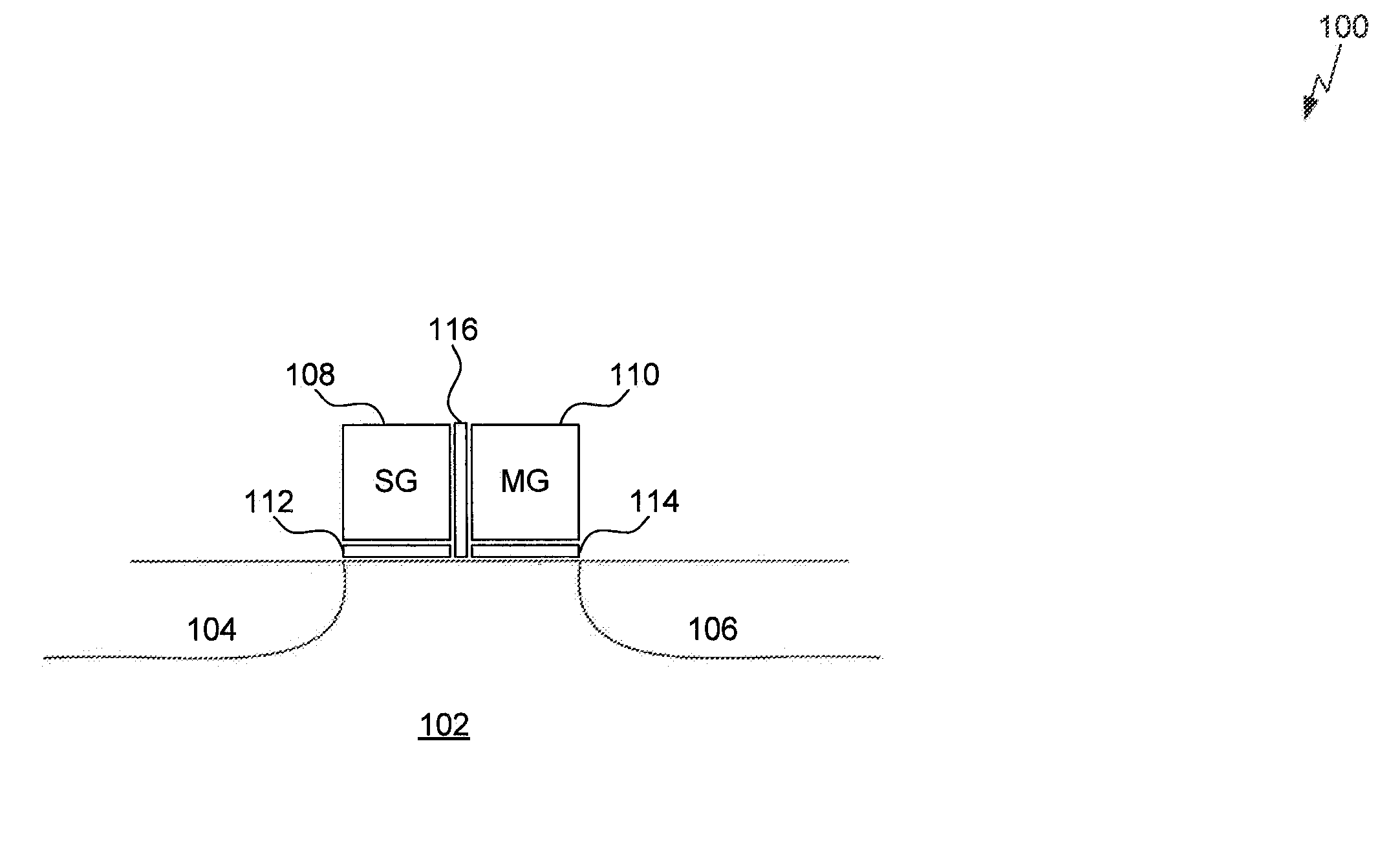
[0024]This specification discloses one or more embodiments that incorporate the features of this invention. The disclosed embodiment(s) merely exemplify the present invention. The scope of the present invention is not limited to the disclosed embodiment(s). The present invention is defined by the claims appended hereto.

[0025]The embodiment(s) described, and references in the specification to “one embodiment,”“an embodiment,”“an example embodiment,” etc., indicate that the embodiment(s) described may include a particular feature, structure, or characteristic, but every embodiment may not necessarily include the particular feature, structure, or characteristic. Moreover, such phrases are not necessarily referring to the same embodiment. Further, when a particular feature, structure, or characteristic is described in connection with an embodiment, it is understood that it is within the knowledge of one skilled in the art to effect such feature, structure, or characteristic in connectio...


PUM


Abstract

A semiconductor device and method of making such device is presented herein. The method includes disposing a gate layer over a dielectric layer on a substrate and further disposing a cap layer over the gate layer. A first transistor gate is defined having an initial thickness substantially equal to a combined thickness of the cap layer and the gate layer. A first doped region is formed in the substrate adjacent to the first transistor gate. The cap layer is subsequently removed and a second transistor gate is defined having a thickness substantially equal to the thickness of the gate layer. Afterwards, a second doped region is formed in the substrate adjacent to the second transistor gate. The first doped region extends deeper in the substrate than the second doped region, and a final thickness of the first transistor gate is substantially equal to the thickness of the second transistor gate.

Description

BACKGROUND[0001]1. Field[0002]The present application relates to the fabrication of split-gate charge trapping memory cells and other field-effect transistors formed in the same substrate.[0003]2. Background Art[0004]A non-volatile memory, such as Flash memory, retains stored data even if power to the memory is removed. A non-volatile memory cell stores data, for example, by storing electrical charge in an electrically isolated floating gate or in a charge-trapping layer underlying a control gate of a field-effect transistor (FET). The stored electrical charge controls the threshold of the FET, thereby controlling the memory state of the cell.[0005]A non-volatile memory cell is programmed using, for example, hot carrier injection to place charge into a storage layer. High drain and gate voltages are used to facilitate the programming process, and the memory cell conducts relatively high current during programming, which can be undesirable in low voltage or low power applications.[00...

Claims


Application Information

Patent Timeline
IPC IPC(8): H01L29/792H01L29/66
CPCH01L29/42344H01L29/792H01L29/66833H01L29/40117H10B43/40H10B43/30H10B43/35H10B99/00
Inventor CHEN, CHUNRAMSBEY, MARKFANG, SHENQING
Owner CYPRESS SEMICON CORP
Features
  • R&D
  • Intellectual Property
  • Life Sciences
  • Materials
  • Tech Scout
  • Unparalleled Data Quality
  • Higher Quality Content
  • 60% Fewer Hallucinations
Learn More