Liquid crystal display device and method for fabricating the same

a liquid crystal display and display device technology, applied in optics, instruments, electrical equipment, etc., can solve the problems of reducing the bonding force, difficult in the related art ffs lcd device to control and low viewing angle characteristics of lcd devices, so as to reduce the margin for a spread width of seal patterns, prevent the spread of seal patterns and alignment layers, and fine seal patterns

Active Publication Date: 2014-06-26
LG DISPLAY CO LTD
View PDF5 Cites 26 Cited by
  • Summary
  • Abstract
  • Description
  • Claims
  • Application Information

AI Technical Summary

Benefits of technology

[0027]Therefore, to overcome those drawbacks of the related art, an aspect of the detailed description is to provide a liquid crystal display (LCD) device, capable of realizing a fine seal pattern by preventing spreading of a seal pattern and alignment layers and reducing a margin for a spread width of the seal pattern, in a manner of forming a seal pattern insertion groove on a non-display region of a lower substrate and forming partition walls for fixing the seal pattern on an upper substrate upon fabricating an FFS mode LCD device, and a fabricating method thereof.

Problems solved by technology

But the LCD device has a low viewing angle characteristic due to the liquid crystal molecules being driven by the vertically formed electric field.
This causes a problem of lowering a bonding force.
As described above, it is difficult in the related art FFS LCD device to control the spreading of the seal pattern formed on the non-display region NA and the spreading of the alignment layer.
Also, it is likely to cause a defect that a cell is not separated during a cell scribing process when a margin is low due to the spreading of the seal pattern.
In addition, in the related art, due to the spreading of the seal pattern, the lower alignment layer and the upper alignment layer are also spread out of their areas to overlap the seal pattern 51, which causes a problem of lowering a bonding force.

Method used


Image

  • Liquid crystal display device and method for fabricating the same
  • Liquid crystal display device and method for fabricating the same
  • Liquid crystal display device and method for fabricating the same

Examples


Embodiment Construction

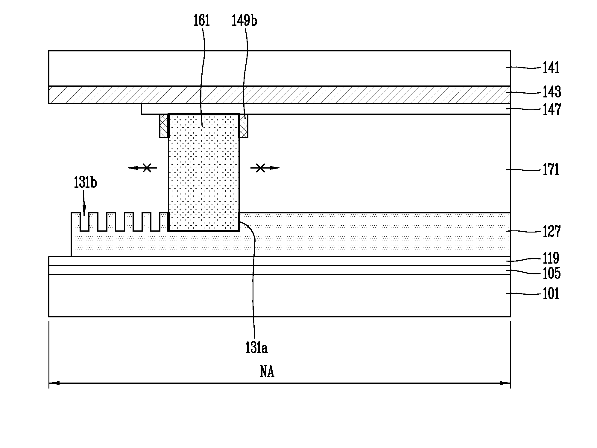
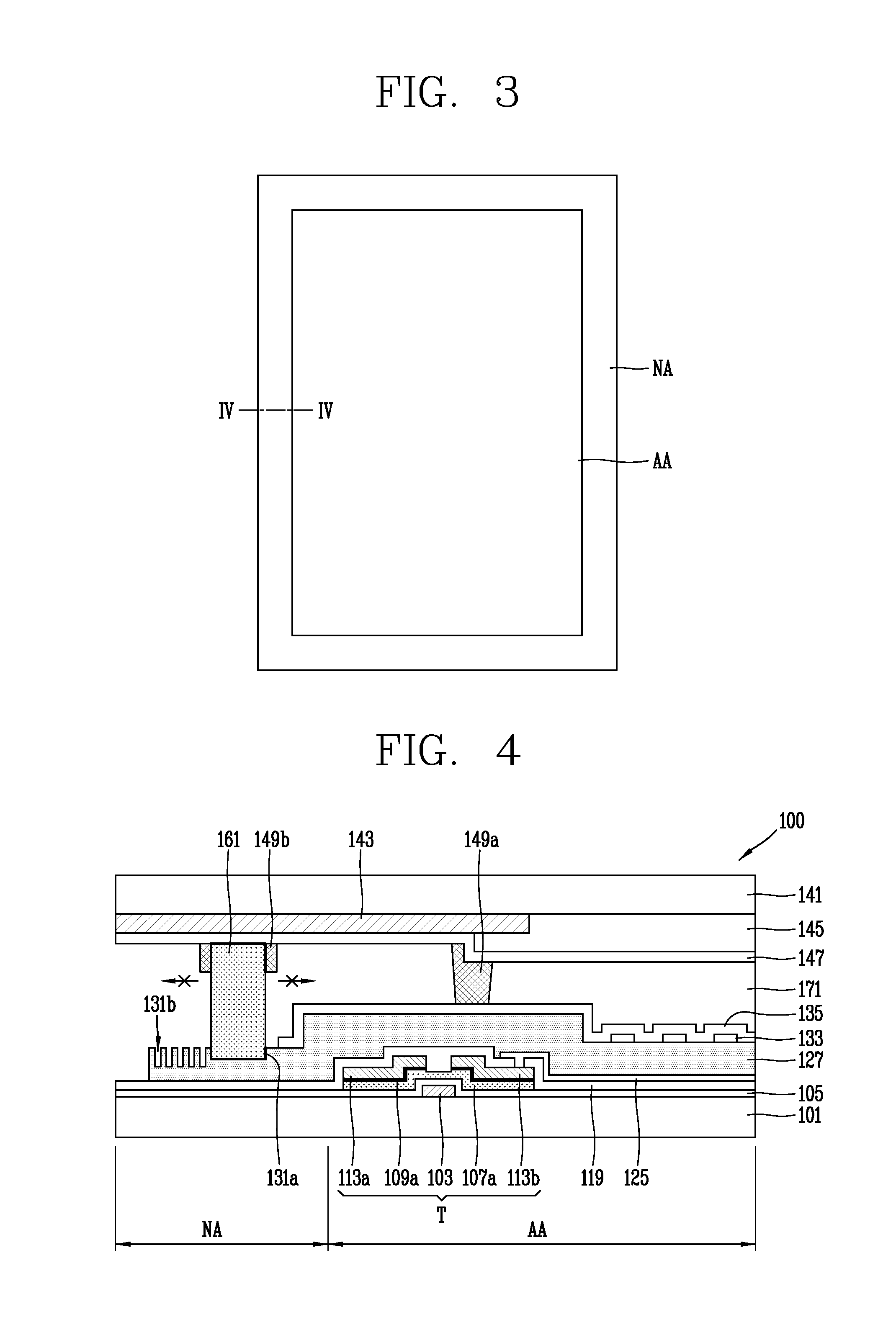
[0041]Description will now be given in detail of a fringe field switching (FFS) mode LCD device according to the exemplary embodiments, with reference to the accompanying drawings. For the sake of brief description with reference to the drawings, the same or equivalent components will be provided with the same reference numbers, and description thereof will not be repeated.

[0042]FIG. 3 is a planar view schematically showing an FFS mode LCD device in accordance with an exemplary embodiment of the present disclosure, and FIG. 4 is a sectional view schematically showing the FFS mode LCD device in accordance with the present disclosure.

[0043]The present disclosure exemplarily illustrates an FFS mode LCD device, but may not be limited to the type. It should be understood that the present disclosure can also be applied to LCD devices and other display devices using different driving methods including an in-plane switching (IPS) mode and a twisted nematic (TN) mode.

[0044]An FFS mode LCD de...


PUM

PropertyMeasurementUnit
photosensitivityaaaaaaaaaa
widthaaaaaaaaaa
distanceaaaaaaaaaa

Abstract

The present disclosure relates to a liquid crystal display device and a fabricating method thereof. The device includes a thin film transistor formed on a lower substrate, a pixel electrode formed on the lower substrate, a planarization layer formed on an entire surface of the lower substrate, a black matrix formed on the upper substrate, a color filter layer formed on a upper substrate, partition walls formed on the upper substrate and forming a space corresponding to a seal pattern insertion groove, a liquid crystal layer interposed between the lower substrate and the upper substrate, and a seal pattern inserted between the seal pattern insertion groove located on the non-display region of the lower substrate and the upper substrate and the partition walls.

Description

CROSS-REFERENCE TO RELATED APPLICATION[0001]This application claims the benefit of Korean Patent Application No. 10-2012-0153659, filed on Dec. 26, 2012, which is hereby incorporated by reference for all purposes as if fully set forth herein.BACKGROUND OF THE DISCLOSURE[0002]1. Field of the Disclosure[0003]This specification relates to a liquid crystal display (LCD) device, and particularly, to an LCD device and a fabricating method thereof.[0004]2. Background of the Disclosure[0005]In general, liquid crystal display (LCD) devices utilize properties of liquid crystals, such as optical anisotropy and polarity. Since the liquid crystal molecules have a long thin structure and an alignment orientation, alignment of the liquid crystal molecules can be controlled by artificial application of an electric field to the liquid crystals.[0006]Accordingly, when the alignment orientation of the liquid crystal molecules is randomly adjusted, light is refracted toward the alignment orientation of...

Claims


Application Information

Patent Timeline
Patent Type & Authority Applications(United States)
IPC IPC(8): G02F1/1339
CPCG02F1/1339G02F1/133345G02F1/1362G02F1/1368G02F1/133512G02F1/133516G02F1/1337G02F1/13394G02F1/13439G02F1/136286G02F2201/123G02F1/133357G02F1/134372
Inventor PARK, MUNGI
Owner LG DISPLAY CO LTD
Why Eureka
Try Eureka