

Light emitting element
a technology of light-emitting elements and electrodes, which is applied in the direction of basic electric elements, electrical apparatus, and semiconductor devices, etc., can solve the problems of insufficient emission, increase of forward voltage (vf), and decrease of emission efficiency, so as to achieve further improvement of emission efficiency
- Summary
- Abstract
- Description
- Claims
- Application Information
AI Technical Summary
Benefits of technology
Problems solved by technology
Method used
Image

Examples
embodiment 1
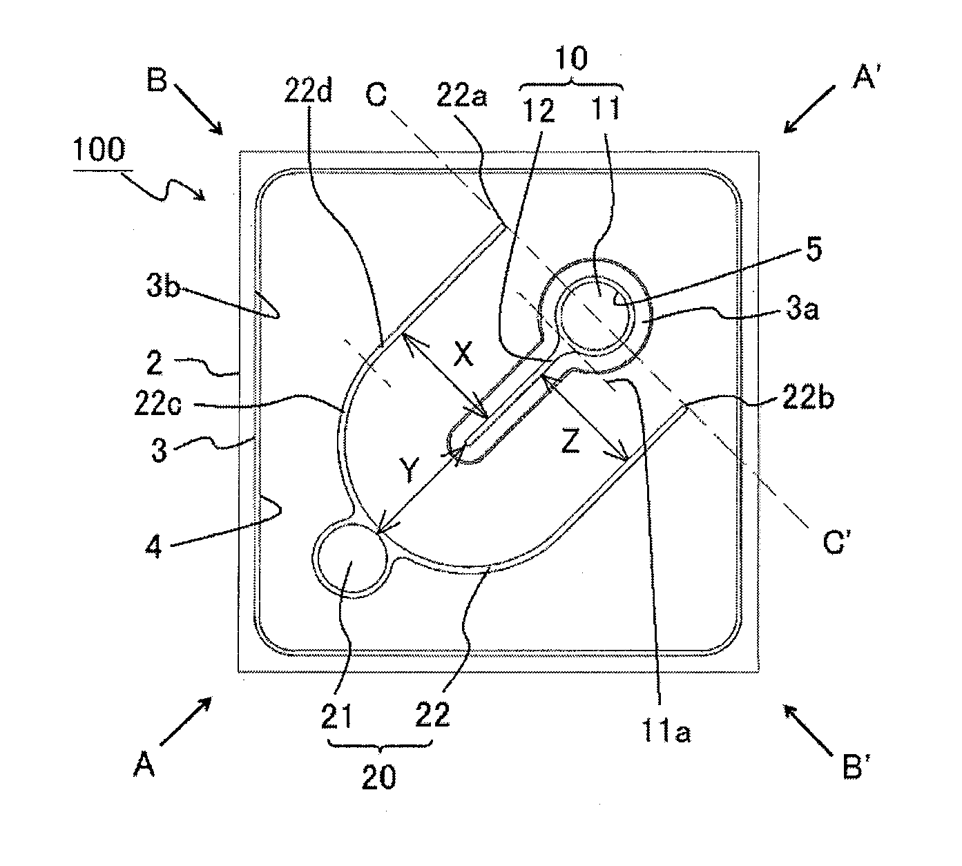
[0072]A light emitting element 100 according to Embodiment 1 includes, as shown in FIG. 1A and FIG. 1B, a substrate 2, a semiconductor layer 3 arranged on the substrate 2, a first electrode 10 disposed on the semiconductor layer 3, and a second electrode 20 arranged over the semiconductor layer 3 and outer periphery of the first electrode 10.
[0073]The semiconductor layer 3 includes a first conductivity-type semiconductor layer 3a (for example, an n-layer), an active layer 3c, and a second conductivity-type semiconductor layer 3b (for example, a p-layer).
[0074]The substrate 2 and the semiconductor layer 3 (particularly, the second conductivity-type semiconductor layer 3b) has an approximately square shape in a plan view. For example, the length of a side of the substrate 2 is 460 μm.
[0075]The first electrode 10 is disposed on the first conductivity-type semiconductor layer 3a which is exposed by removing a part of the second conductivity-type semiconductor layer 3b and the active lay...
example 1 of embodiment 1
Variant Example 1 of Embodiment 1
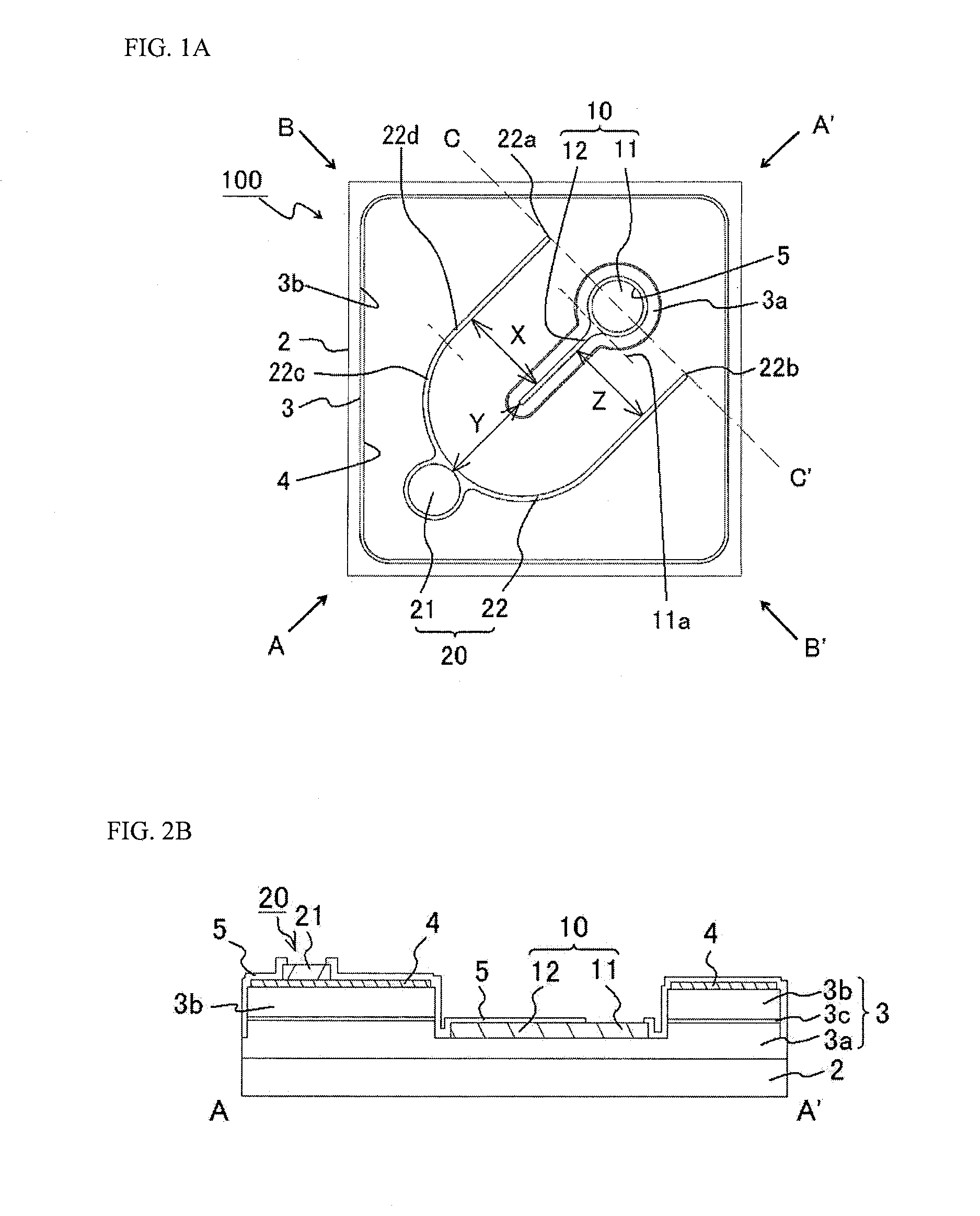
[0082]Also, as shown in FIG. 1C, a light emitting element 101 has a substantially similar structure as the light emitting element 100, as the light emitting element 101 includes a substrate 2, a semiconductor layer 3 disposed on the substrate 2, a first electrode 10 disposed on the semiconductor layer 3, and a second electrode 20 arranged over the semiconductor layer 3 and at outer periphery of the first electrode 10.
[0083]Also, the entire of the first connecting portion 11 is disposed closer side to the second connecting portion 21 than the a straight line C-C′ intersecting the two tip portions 22a and 22b of the second portions 22d of the respective second extending portions 22. As shown in FIG. 1C, the straight line C-C′ is spaced apart from the first electrode 10. With this arrangement, the distance between the first connecting portion 11 and the second connecting portion 21 can be reduced, so that resistance between the first connecting portion ...
example 2 of embodiment 1
Variant Example 2 of Embodiment 1
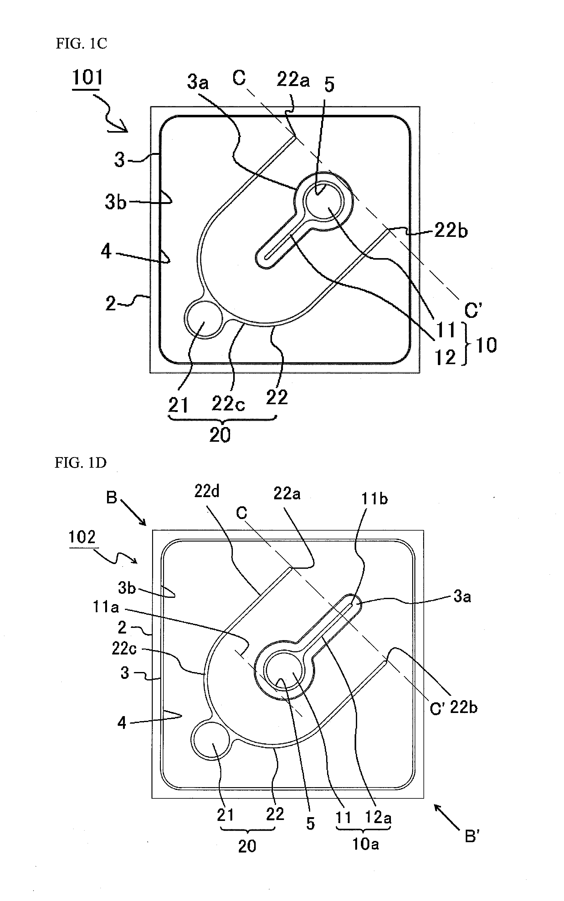
[0084]Also, as shown in FIG. 1D, a light emitting element 102 has a substantially similar structure as the light emitting element 100, as the light emitting element 102 includes a substrate 2, a semiconductor layer 3 disposed on the substrate 2, a first electrode 10a disposed on the semiconductor layer 3, and a second electrode 20 arranged over the semiconductor layer 3 and at outer periphery of the first electrode 10a.
[0085]The first electrode 10a includes a first connecting portion 11 and a first auxiliary extending portion 12a extending from the first connecting portion 11.
[0086]The first connecting portion 11 is arranged on the second diagonal line B-B′ and the center portion of the first connecting portion 11 is on the second diagonal line B-B′. Thus, the first connecting portion 11 is arranged so that the end portion 11a of the first connecting portion 11 which is close to the second connecting portion 21 is closer side to the second connectin...
PUM
 Abstract
Description
Claims
Application Information