

Finfet with dielectric isolation by silicon-on-nothing and method of fabrication
a technology of silicon-on-nothing and dielectric isolation, applied in the direction of basic electric elements, electrical equipment, semiconductor devices, etc., can solve the problems of degrading electrical performance and high manufacturing cos
- Summary
- Abstract
- Description
- Claims
- Application Information
AI Technical Summary
Benefits of technology
Problems solved by technology
Method used
Image

Examples
Embodiment Construction
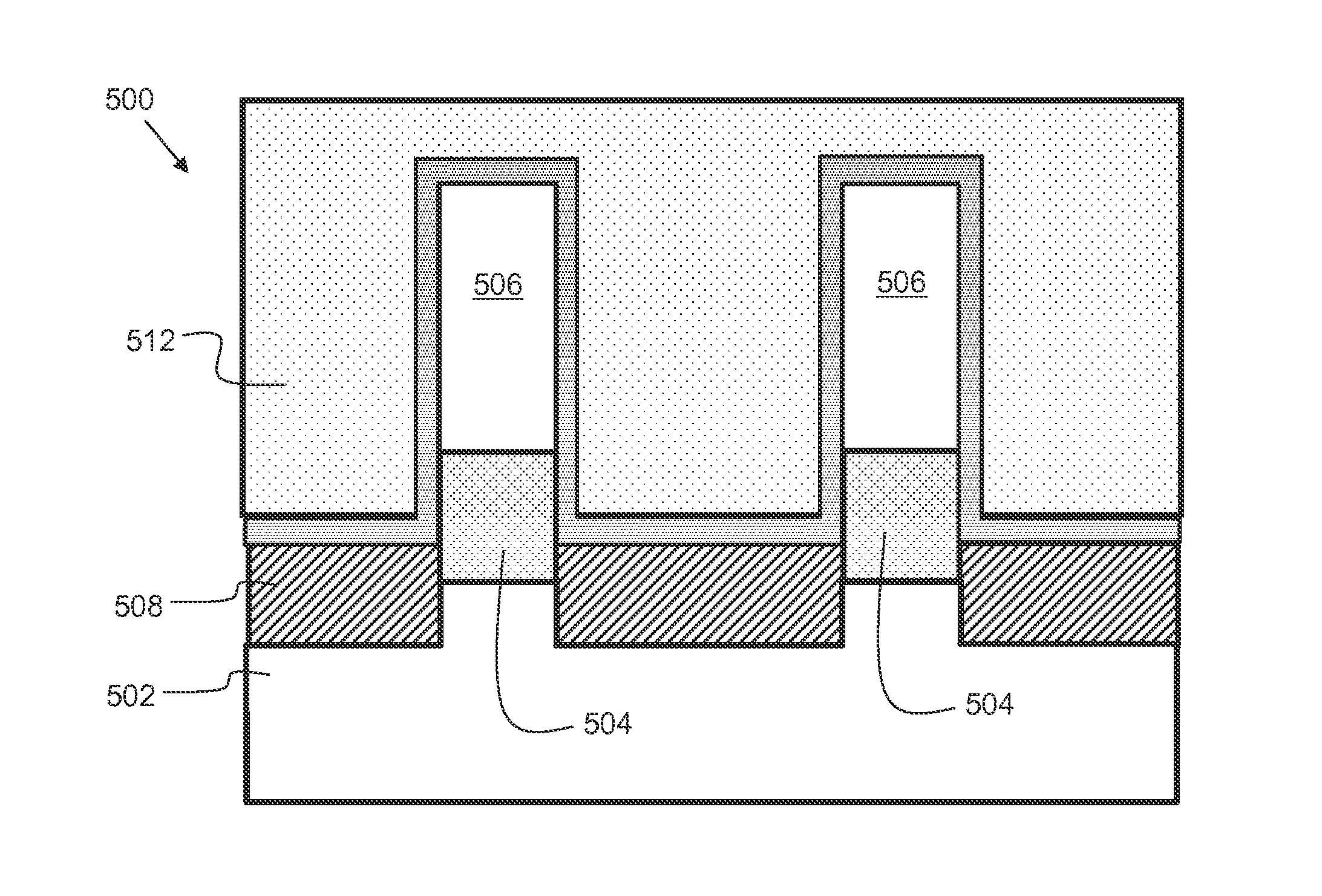
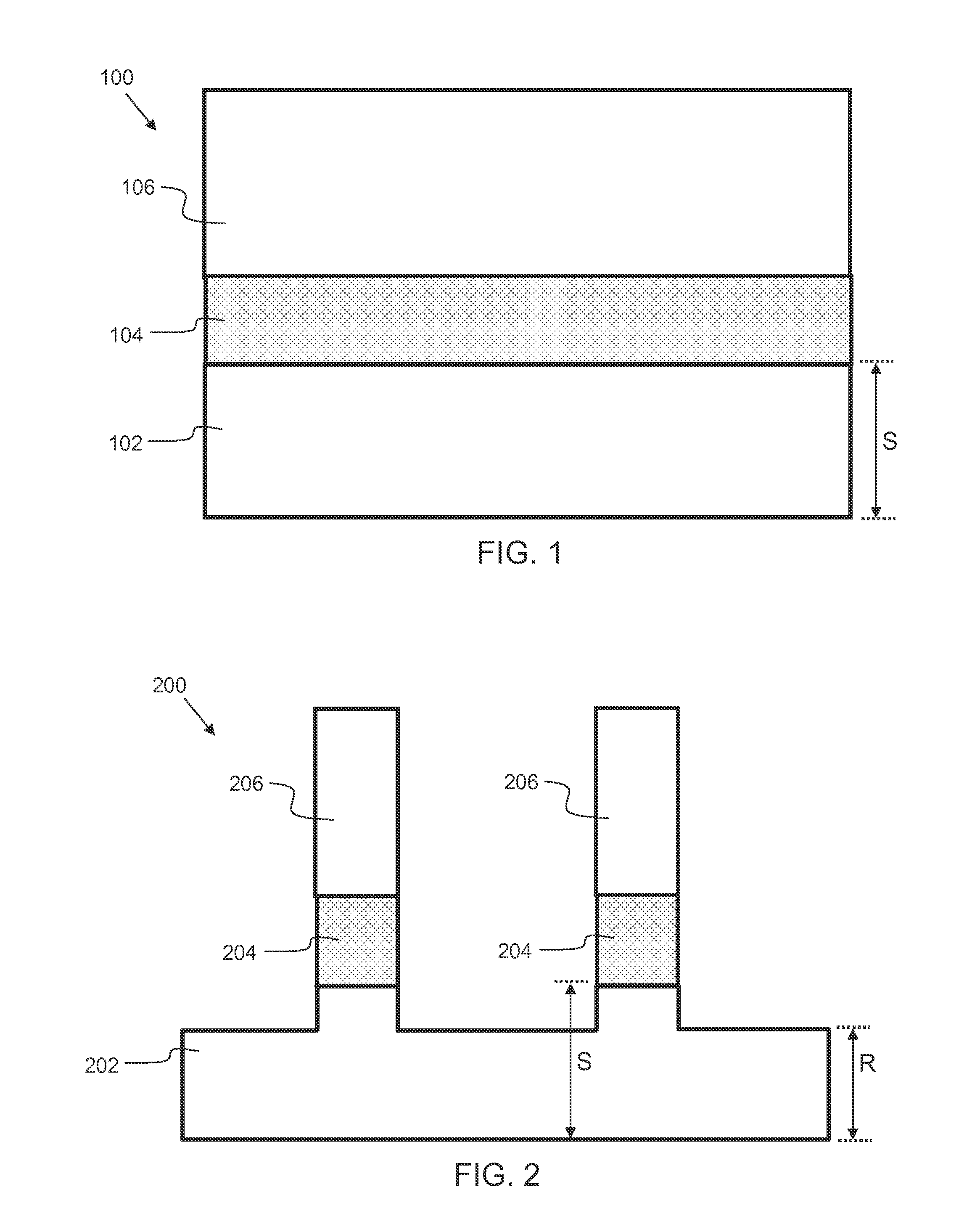
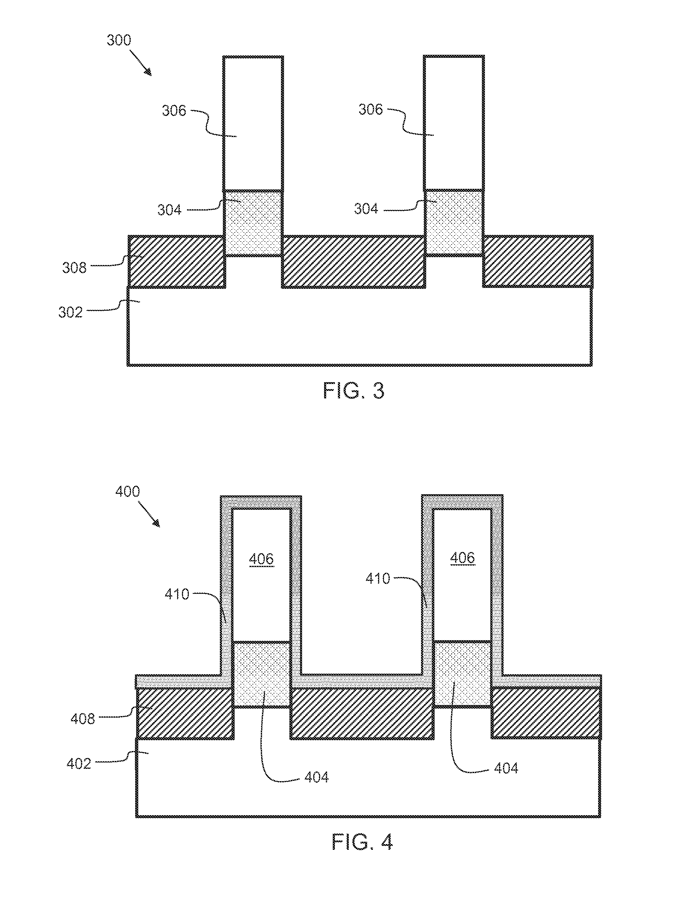
[0034]Silicon-on-nothing (SON) is a common approach to form a dielectric isolated silicon fin. One practical problem in the current SON process flow is that of silicon fin loss when removing a sacrificial layer to form the cavity where dielectric is to be filled. Even when selective etch techniques are used, they are not perfectly selective, and hence, fin etching occurs, resulting in a loss of fin material. This loss limits the critical dimension of the fin devices that can be used with the current SON process flow.
[0035]Within this disclosure, when an element as a layer, region, substrate, or wafer is referred to as being “on” or “over” another element, it can be directly on the other element or intervening elements may also be present. In contrast, when an element is referred to as being “directly on” or “directly over” another element, there are no intervening elements present. It will also be understood that when an element is referred to as being “connected” or “coupled” to an...
PUM
 Abstract
Description
Claims
Application Information