Touch panel and manufacturing method thereof

a technology of touch panel and manufacturing method, which is applied in the field of touch panel, can solve problems such as color shift in the touch panel, and achieve the effects of improving the visual effect of the touch panel, avoiding color shift problems, and improving the uniformity of the entire touch panel

Inactive Publication Date: 2014-07-31
AU OPTRONICS CORP
View PDF9 Cites 16 Cited by
  • Summary
  • Abstract
  • Description
  • Claims
  • Application Information

AI Technical Summary

Benefits of technology

[0012]Accordingly, the present invention is directed to a touch panel, wherein the problem of color shift is effectively overcome and accordingly the visual effect of the touch panel is improved.
[0013]The present invention is directed to a touch panel having good transmittance, and a good display quality can be achieved when the touch panel is applied in a display device.
[0032]According to the present invention, in a touch panel having a double-layered sensing pad structure, dummy sensing pads are disposed on each layer corresponding to the sensing pads on the other layer for compensating the color shift of the touch panel and to improve the visual effect thereof. Additionally, according to the present invention, the sensing pads may also be formed on the same plane so as to form a touch panel having a single-layered sensing pad structure, and various patterns for connecting the sensing pads in different directions are provided. Since the sensing pads are all disposed on the same plane, the problem of color shift is avoided and the display uniformity of the entire touch panel is improved. On the other hand, in the present invention, dummy patterns may be disposed between adjacent sensing pads in order to further improve the visual effect of the touch panel; Or, at least one opening may be formed on each sensing pad to form a hollow portion on the sensing pad so that the visual effect of the touch panel, and accordingly the transmittance thereof, can be further improved.

Problems solved by technology

All of foregoing facts may cause the problem of color shift in the touch panel.

Method used


Image

  • Touch panel and manufacturing method thereof
  • Touch panel and manufacturing method thereof
  • Touch panel and manufacturing method thereof

Examples


Embodiment Construction

[0044]Reference will now be made in detail to the present preferred embodiments of the invention, examples of which are illustrated in the accompanying drawings. Wherever possible, the same reference numbers are used in the drawings and the description to refer to the same or like parts.

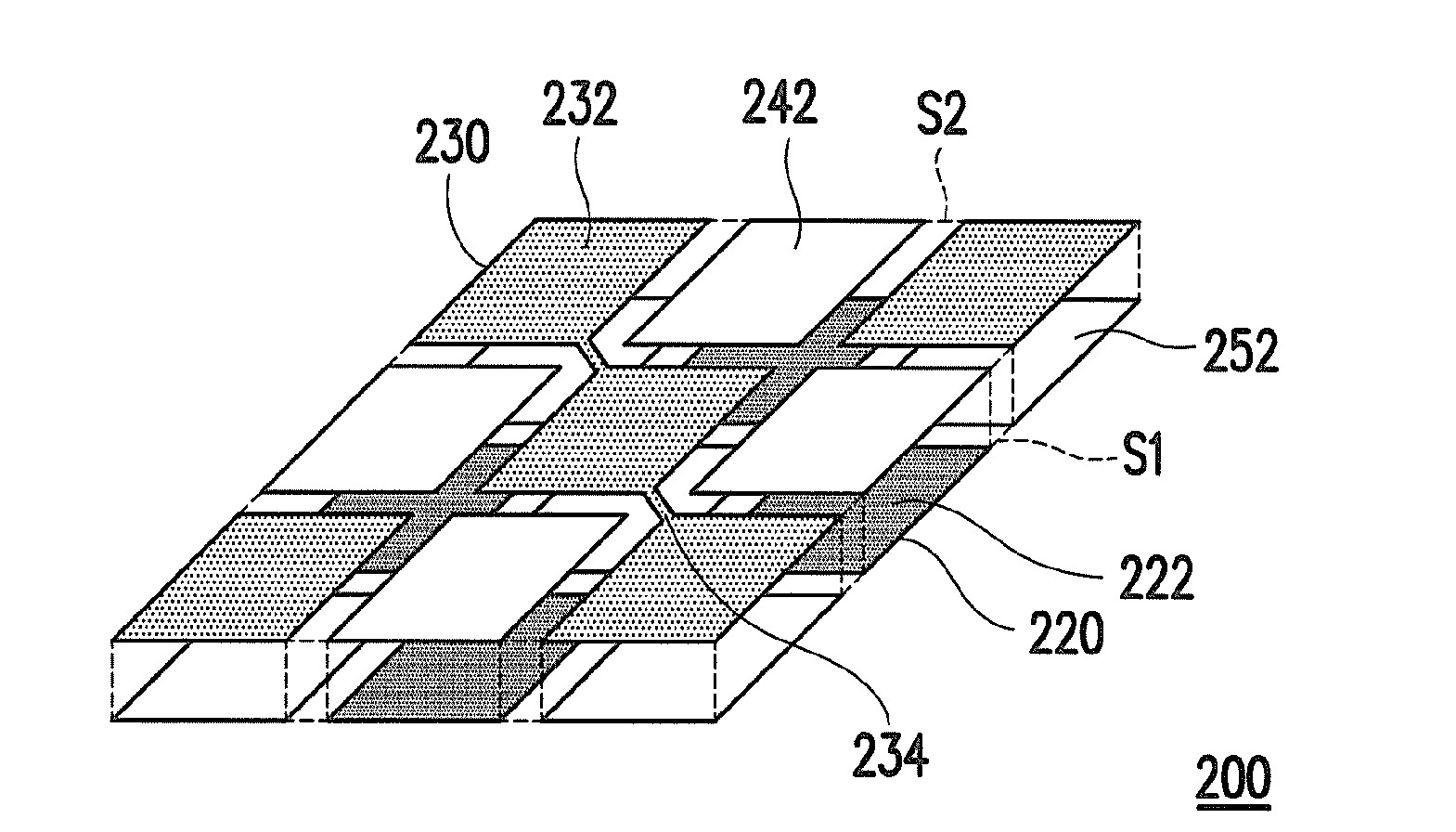
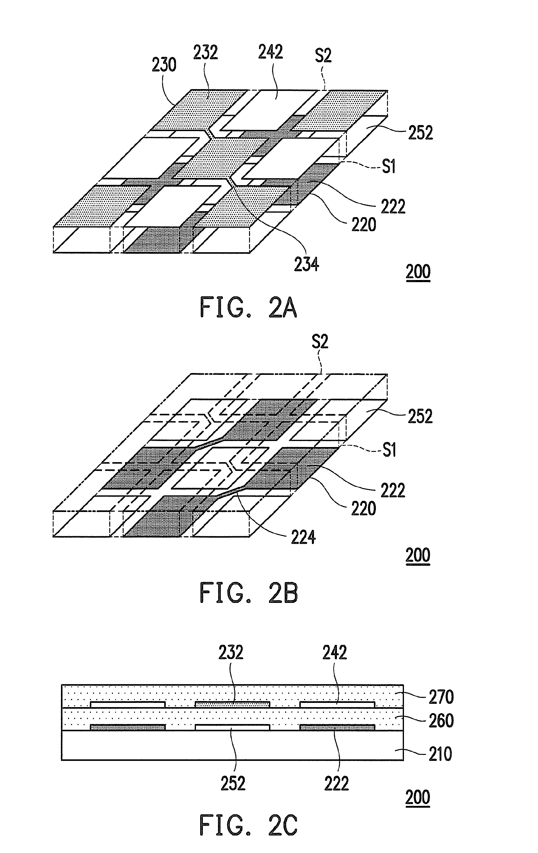
[0045]FIGS. 2A˜2C illustrate a touch panel according to an embodiment of the present invention, wherein FIG. 2A is a 3-dimensional view of the touch panel, FIG. 2B is a perspective view of the touch panel, and FIG. 2C is a cross-sectional view of the touch panel. For the convenience of description, FIG. 2A and FIG. 2B illustrate only the sensing pad structure in the touch panel, whileFIG. 2C illustrates some other layers, such as a substrate and other dielectric layers, of the touch panel.

[0046]Referring to FIGS. 2A˜2C, in the present embodiment, the touch panel 200 has a double-layered sensing pad structure and which includes a substrate 210, a first sensing serial 220, a second sensing serial 230, ...


PUM


Abstract

A touch panel and a manufacturing method thereof are provided. The touch panel has a double-layered sensing pad structure or a single-layered sensing pad structure. In the double-layered sensing pad structure, the sensing pads in each layer have corresponding dummy sensing pads in the other layer for compensating the difference of transmittance. In the single-layered sensing pad structure, the sensing pads are coplanar so that the problem of color shift can be overcome and the visual effect of the touch panel can be improved.

Description

CROSS-REFERENCE TO RELATED APPLICATION[0001]This is a continuation application of and claims the priority benefit of U.S. patent application Ser. No. 12 / 132,625 filed on Jun. 4, 2008, now pending, which claims the priority benefit of Taiwan application serial no. 96136550, filed on Sep. 29, 2007. The entirety of each of the above-mentioned patent applications is hereby incorporated by reference herein and made a part of specification.BACKGROUND OF THE INVENTION[0002]1. Field of the Invention[0003]The present invention generally relates to a touch panel and a manufacturing method thereof, in particular, to a touch panel having improved visual effect and a manufacturing method thereof.[0004]2. Description of Related Art[0005]Along with the development of electronics industry, the designs of digital products, such as mobile phones, personal digital assistants (PDAs), notebook computers, and tablet computers, are all going towards convenience, multi-functionality, and attractive appeara...

Claims


Application Information

Patent Timeline
Patent Type & Authority Applications(United States)
IPC IPC(8): G06F3/041
CPCG06F3/041G06F3/0416G06F2203/04103G06F2203/04111G06F3/0446G06F3/0443G06F3/0445G06F3/0448G06F3/0412
Inventor WU, YUAN-CHUNLEE, HSIN-HUNGMA, MEI-SHENGYANG, TUN-CHUNLEE, SEOK-LYULHSIEH, YAO-JEN
Owner AU OPTRONICS CORP
Why Eureka
Try Eureka