Touch display apparatus

a display device and touch technology, applied in the field of display devices, can solve the problems of reducing the touch effect of the touch display device, bending noise, lagging noise, etc., and achieve the effect of excellent touch

Active Publication Date: 2019-12-17
AU OPTRONICS CORP
View PDF4 Cites 2 Cited by
  • Summary
  • Abstract
  • Description
  • Claims
  • Application Information

AI Technical Summary

Benefits of technology

[0005]A touch display apparatus with excellent touch effect is provided in the invention.
[0016]Based on the foregoing, the spacer is disposed inside the first opening of the touch-sensing electrode in an orthogonal projection direction. A distance D is defined between an outline of an orthogonal projection of the spacer on the first substrate and an outline of an orthogonal projection of the first opening on the first substrate, and D≥5 μm. In other words, a sufficient distance is maintained between an edge of the touch-sensing electrode and the spacer. Since the distance between the edge of the touch-sensing electrode and the spacer is sufficiently large, capacitance between the touch-sensing electrode and the spacer is extremely low. As a result, before or after the touch display apparatus is pressed by an object, that is to say before or after the spacer is squeezed, the capacitance between the touch-sensing electrode and the spacer has a very limited influence on determining a touch location. The lagging noise is thus reduced and the touch effect is improved.

Problems solved by technology

The capacitance between the touch-sensing electrode and the members (e.g. the spacer) on the lower substrate of the display panel changes overly drastically and results in bending noise.
The time required for the members to recover to their original statuses further results in lagging noise.
Both the bending noise and the lagging noise reduce the touch effect of the touch display apparatuses.

Method used


Image

  • Touch display apparatus
  • Touch display apparatus
  • Touch display apparatus

Examples


Embodiment Construction

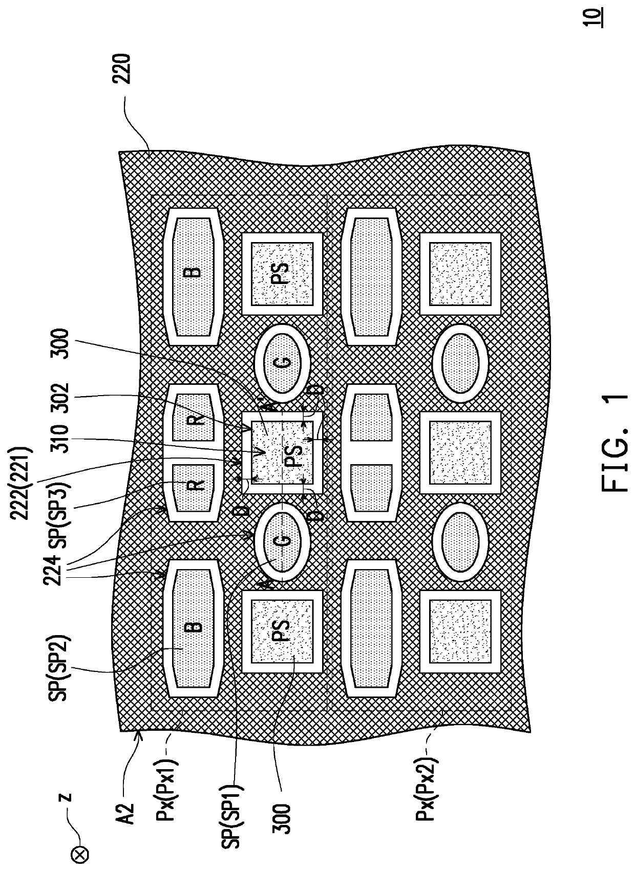
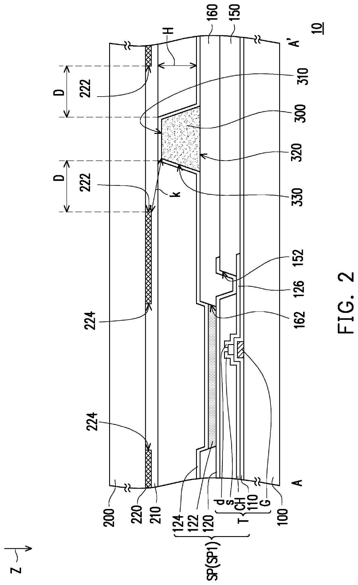
[0022]FIG. 1 is a top view of part of a touch display apparatus according to an exemplary embodiment of the invention. FIG. 2 is a cross-sectional view of part of a touch display apparatus according to an exemplary embodiment of the invention. A cut plane of a touch display apparatus 10 illustrated in FIG. 2 is correspondent to a cut line A-A′ in FIG. 1.

[0023]Referring to FIG. 1 and FIG. 2, the touch display apparatus 10 includes a first substrate 100, a plurality of sub-pixels SP, a spacer 300, a second substrate 200, and a touch-sensing electrode 220. The plurality of sub-pixels SP are disposed on the first substrate 100. According to this exemplary embodiment, each sub-pixel SP among the plurality of sub-pixels SP includes a thin-film transistor T, a first electrode 120 electrically connected to the thin-film transistor T, a light-emitting pattern 122 disposed on the first electrode 120, and a second electrode 124 covering the light-emitting pattern 122. The thin-film transistor ...


PUM


Abstract

A touch display apparatus including a first substrate, a first sub-pixel, a spacer, a second substrate, and a touch-sensing electrode is provided. The first sub-pixel is disposed on the first substrate. The spacer is disposed on the first substrate. The touch-sensing electrode is disposed on the second substrate and has a first opening. The spacer is located inside the first opening in an orthogonal projection direction. A distance D is defined between an outline of an orthogonal projection of the spacer on the first substrate and an outline of an orthogonal projection of the first opening on the first substrate, and D≥5 μm.

Description

CROSS-REFERENCE TO RELATED APPLICATION[0001]This application claims the priority benefit of Taiwan application serial no. 106145479, filed on Dec. 25, 2017. The entirety of the above-mentioned patent application is hereby incorporated by reference herein and made a part of this specification.BACKGROUND OF THE INVENTIONField of the Invention[0002]The invention relates to a display apparatus, and particularly to a touch display apparatus.Description of Related Art[0003]Touch display apparatuses can generally be divided into out-cell types, on-cell types, and in-cell types according to the relative location of the touch-sensing electrode and display panel. Comparing with the out-cell and on-cell types of touch display apparatuses, the in-cell types of touch display apparatuses have the advantages in being thinned more easily. The in-cell types of touch display apparatuses are thus broadly applied in various electronic devices.[0004]When the upper substrate of an in-cell type of touch d...

Claims


Application Information

Patent Timeline
Patent Type & Authority Patents(United States)
IPC IPC(8): G06F3/044G06F3/041H01L27/32
CPCH01L27/3246G06F3/044G06F3/0412H01L27/323H01L27/3262G06F2203/04112H10K59/40G06F3/0443H10K59/352H10K59/1213H10K59/122H10K50/8428
Inventor LAI, CHUN-CHICHU, CHIA-HSIENYEH, CHIA-YUANCHEN, KUAN-TINGLAU, CHEE-WAIHSIEH, AN-HSIUNGLIN, FENG-SHENGWANG, TSANG-HONG
Owner AU OPTRONICS CORP
Why Eureka
Try Eureka