Method for manufacturing a component interconnect board

a technology of light-emitting diodes and interconnect boards, which is applied in the direction of laminating printed circuit boards, lighting and heating apparatus, and supporting devices, etc. it can solve the problems of costing extra time and energy, growing a thicker layer, and little room left to have a cost down on for example the housing parts, so as to achieve faster and more economical, material-efficient

Inactive Publication Date: 2014-08-07
SIGNIFY HLDG BV
View PDF7 Cites 1 Cited by
  • Summary
  • Abstract
  • Description
  • Claims
  • Application Information

AI Technical Summary

Benefits of technology

[0007]In view of the above, an object of the invention is to at least alleviate the problems discussed above. In particular, an object is to provide a method for manufacturing a component interconnect board in a more material efficient, faster and more economical manner.

Problems solved by technology

Firstly, the LED costs are decreasing, and secondly, in many LED luminaire designs, there is little room left to have a cost down on for example the housing parts.
Further, with respect to material utilization, there is little flexibility in playing with the essential and valuable conductor layer properties.
Growing a thicker layer, for better heat management, also cost extra time and energy.
In addition to the standard PCB type of L2 interconnect described above, there are many other types of L2 interconnects, which are mostly not relevant for reasons of high cost and complexity.
There are some typical drawbacks to this approach.
Firstly with creating the final circuitry the initial lead-frame will lose its mechanical integrity literally falling apart.
Furthermore in general these types of solutions do not provide for the necessary electronic insulation requirements whereas dielectrics are not or only applied in limited areas.
Prescribed creepage and clearance distances are difficult to manage or incorporate into the L2 interconnect design and must mostly be managed on a luminaire / system level.

Method used


Image

  • Method for manufacturing a component interconnect board
  • Method for manufacturing a component interconnect board
  • Method for manufacturing a component interconnect board

Examples


Embodiment Construction

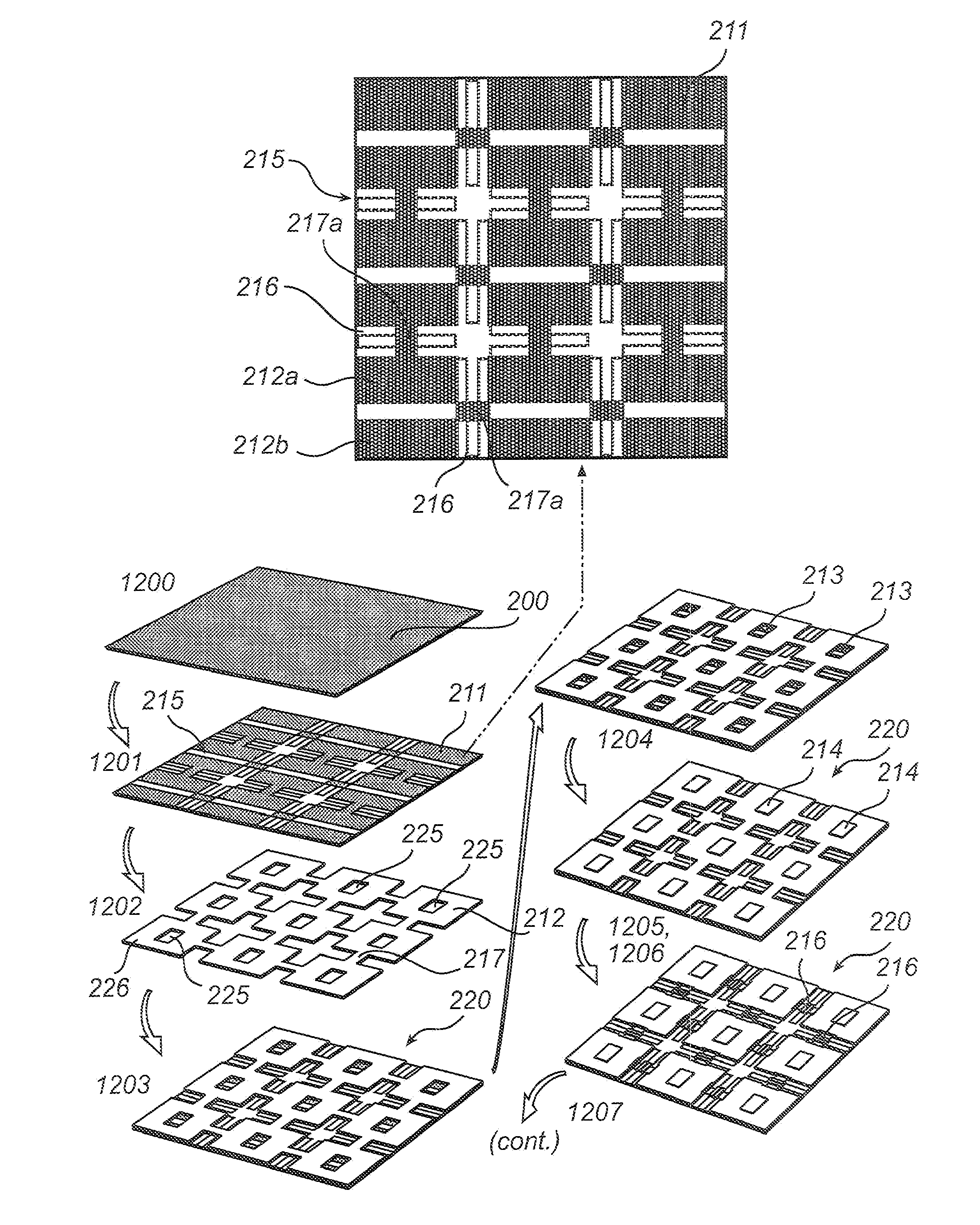
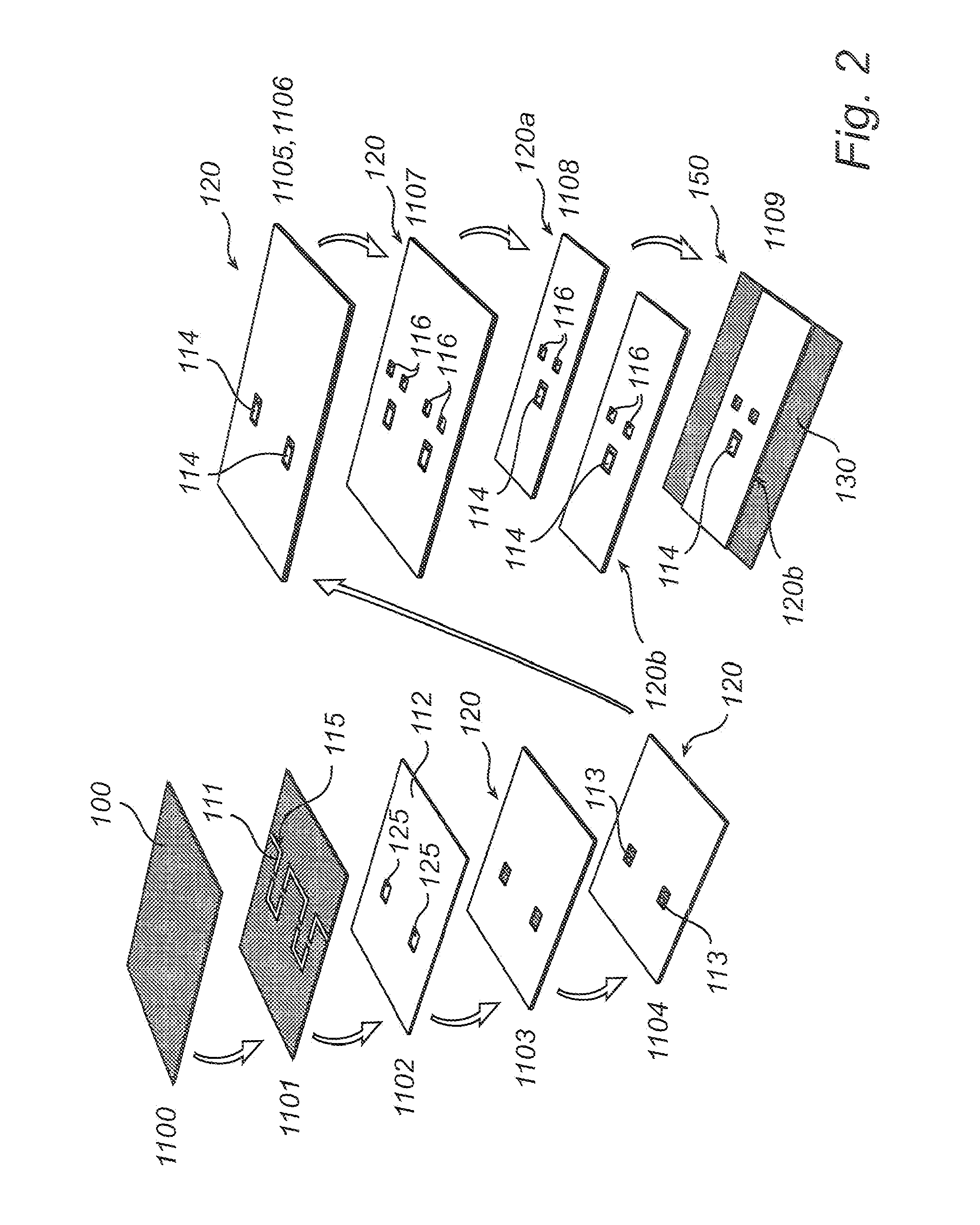
[0029]Exemplifying embodiments of the method for manufacturing a component interconnect board according to the present invention is now described with reference toFIGS. 2, 3 and 4. The steps of the method are shown as a numerical sequence, however some of the steps may be performed in another order.

[0030]With reference now to FIG. 2, and starting at step 1100, a conductor sheet 100 is initially provided. The conductor sheet 100 is preferably selected amongst a group of metal sheet materials comprising copper and silver. The conductor sheet 100 is in step 1101 pre-cut to apply a first predetermined pattern 115 corresponding to a specific electronic layout while still maintaining the necessary integrity.

[0031]In a parallel step 1102, a solder resist sheet 112 is pre-cut to provide a second predetermined pattern, here defining openings 125 for defining solder areas, while still maintaining the necessary integrity.

[0032]The maintained integrity of the patterned conductor sheet 111 and t...


PUM

PropertyMeasurementUnit
thickaaaaaaaaaa
mechanical deformationaaaaaaaaaa
optical propertiesaaaaaaaaaa

Abstract

There is provided a method for manufacturing a component interconnect board (150) comprising a conductor structure for providing electrical circuitry to at least one component (114) when mounted on the component board, the method comprising providing a conductor sheet (100) with a first predetermined pattern (115), providing a solder resist sheet (112) with a second predetermined pattern for defining solder areas (125) of the component board, forming a subassembly (120) by laminating the solder resist sheet on top of the conductor sheet, applying solder onto the subassembly, placing the at least one component onto the subassembly, performing soldering, and laminating the subassembly to a substrate (130). The solder resist sheet is further arranged to act as a carrier for the conductor sheet.

Description

TECHNICAL FIELD[0001]The present invention generally relates to the field of light emitting diode luminaires, and more particularly to a method for manufacturing a component interconnect board for light emitting diode luminaires.BACKGROUND OF THE INVENTION[0002]In the cost breakdown of light emitting diode (LED) luminaires, the component to circuitry interconnect solution, or when the component is part of the circuitry, herein under referred to as a level two (L2) interconnect, is becoming increasingly important because of two main reasons. Firstly, the LED costs are decreasing, and secondly, in many LED luminaire designs, there is little room left to have a cost down on for example the housing parts. Both reasons lead to a relative increase of importance of the L2 interconnect on the total system costs.[0003]FIG. 1 schematically illustrates a typical L2 interconnect in which a component, here a packaged LED 10, is interconnected with a LED board 50 being a printed circuit board, PC...

Claims


Application Information

Patent Timeline
Patent Type & Authority Applications(United States)
IPC IPC(8): H05K3/30F21V21/002
CPCH05K3/303H05K2203/04H05K2203/1545F21V21/002H05K1/0283H05K3/202H05K2201/09263H05K2201/10106H01L25/0753H01L2924/0002H05K13/046H05K1/05Y10T29/49144H01L2924/00H05K1/0209H05K1/0284H05K3/0058H05K3/0097H05K2201/09781H05K2203/175F21K9/90H01L27/153H01L33/62
Inventor DINGEMANS, ANTONIUS PETRUS MARINUS
Owner SIGNIFY HLDG BV
Why Eureka
Try Eureka