Method of manufacturing photoelectric conversion device

a technology of photoelectric conversion and manufacturing method, which is applied in the manufacture of final products, testing/measurement of semiconductor/solid-state devices, and basic electric elements. it can solve the problems of increasing the cost of manufacturing photoelectric conversion elements, affecting the efficiency of production lines, and affecting the production efficiency of the entire production line. achieve excellent photoelectric conversion characteristics, reduce production cost, and improve production efficiency

Inactive Publication Date: 2014-09-04
SHARP KK
View PDF7 Cites 0 Cited by
  • Summary
  • Abstract
  • Description
  • Claims
  • Application Information

AI Technical Summary

Benefits of technology

[0022]According to the method of manufacturing a photoelectric conversion device of the present invention, semiconductor layers are formed within the same reaction chamber, so that a photoelectric conversion device having excellent photoelectric conversion characteristics can be manufactured at low cost and with high efficiency.

Problems solved by technology

In such a manufacturing process, however, the cost for manufacturing the photoelectric conversion element is increased due to an increase in cost for a semiconductor layer manufacturing apparatus represented by the plasma CVD apparatus that is a basic apparatus for manufacturing a device.
This is one of obstacles to widespread proliferation of such a photoelectric conversion element.
Accordingly, there is a disadvantage that the entire production line is stopped even though maintenance is required for only one film formation chamber in which an i-type silicon photoelectric conversion layer is formed.
However, since the manufacturing apparatus in this multi-chamber system includes a plurality of substrate flow lines through the intermediate chamber, it is inevitable that the mechanical structure in the intermediate chamber becomes complicated.
For example, the mechanism for transferring the substrate while maintaining airtightness between the intermediate chamber and each film formation chamber becomes complicated and expensive.
There also occurs a problem that the number of film formation chambers arranged around the intermediate chamber is limited in terms of space.

Method used


Image

  • Method of manufacturing photoelectric conversion device
  • Method of manufacturing photoelectric conversion device
  • Method of manufacturing photoelectric conversion device

Examples


first embodiment

Photoelectric Conversion Device

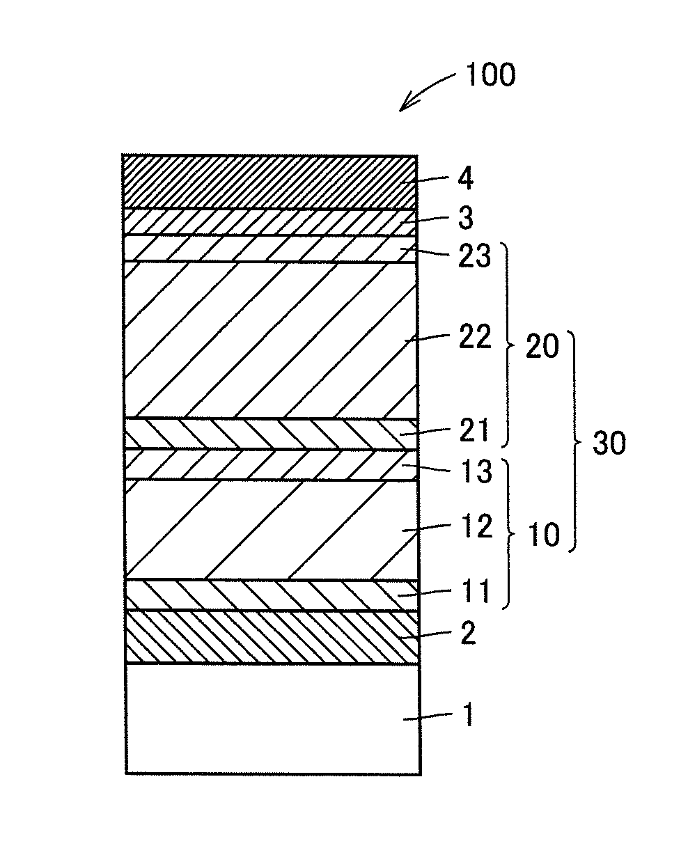
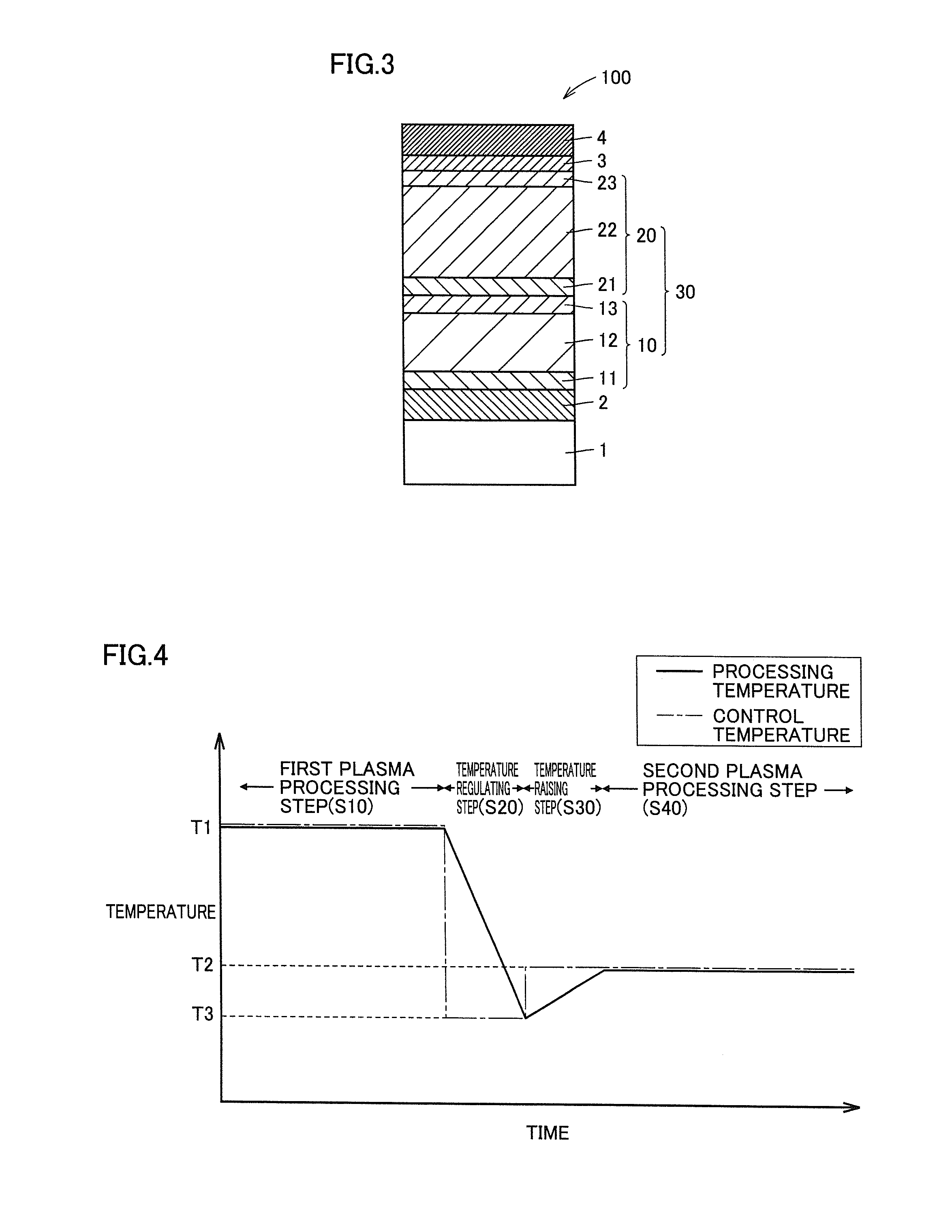
[0044]FIG. 3 is a cross-sectional view schematically showing the configuration of a photoelectric conversion device manufactured by the manufacturing method according to the present embodiment. A photoelectric conversion device 100 shown in FIG. 3 includes a first photoelectric conversion body 10, a second photoelectric conversion body 20, a conductive film 3, and a metal electrode 4 on a transparent conductive film 2 formed on a substrate 1. First photoelectric conversion body 10 is an amorphous pin structure stacked body formed by stacking a first p-type semiconductor layer 11, an i-type amorphous silicon-based photoelectric conversion layer 12 and a first n-type semiconductor layer 13 in this order. Second photoelectric conversion body 20 is a microcrystalline pin structure stacked body formed by stacking a second p-type semiconductor layer 21, an i-type microcrystalline silicon-based photoelectric conversion layer 22 and a second n-type semiconduct...

example 1a

[0058]According to the manufacturing method of the present embodiment, a photoelectric conversion device was produced on the conditions that the power density per electrode unit in the first plasma processing step (S10) was set at 0.068 W / cm2 and the power density per electrode unit in the second plasma processing step (S40) was set at 0.225 W / cm2.

[0059]FIG. 4 is a graph showing changes in the control temperature and the actual processing temperature from the first plasma processing step (S10) to the second plasma processing step (S40) in the present example. In FIG. 4, the horizontal axis shows time while the vertical axis shows a temperature. In FIG. 4, the alternate long and short dashed line shows a control temperature while the solid line shows an actual processing temperature. The processing temperature, that is, the temperature of an anode, was measured by a thermocouple.

[0060]As shown in FIG. 4, the control temperature was set at T1 in the first plasma processing step (S10)....

example 1b

[0062]According to the manufacturing method of the present embodiment, a photoelectric conversion device was produced on the conditions that the power density per electrode unit in the first plasma processing step (S10) was set at 0.068 W / cm2 and the power density per electrode unit in the second plasma processing step (S40) was set at 0.300 W / cm2.

[0063]FIG. 5 is a graph showing changes in the control temperature and the processing temperature from the first plasma processing step (S10) to the second plasma processing step (S40) in the present example. In FIG. 5, the alternate long and short dashed line shows a control temperature while the solid line shows an actual processing temperature. The processing temperature, that is, the temperature of an anode, was measured by a thermocouple.

[0064]As shown in FIG. 5, in the second plasma processing step (S40), since the power density was relatively high and the substrate was readily heated by radio-frequency discharge, the processing temp...


PUM

PropertyMeasurementUnit
pressureaaaaaaaaaa
pressureaaaaaaaaaa
pressureaaaaaaaaaa

Abstract

The present invention provides a method of manufacturing a photoelectric conversion device for forming a semiconductor layer on a substrate by the plasma CVD method. The method includes a first plasma processing step in which a processing temperature reaches a first temperature; a second plasma processing step in which the processing temperature reaches a second temperature; a temperature regulating step of lowering the processing temperature to a third temperature lower than the first temperature and the second temperature after the first plasma processing step and before the second plasma processing step; and a temperature raising step of raising the processing temperature from the third temperature to the second temperature. The first plasma processing step, the temperature regulating step, the temperature raising step, and the second plasma processing step are carried out within the same reaction chamber.

Description

TECHNICAL FIELD[0001]The present invention relates to a method of manufacturing a photoelectric conversion device formed by stacking a plurality of photoelectric conversion bodies.BACKGROUND ART[0002]In recent years, attention has been paid to a thin-film photoelectric conversion element formed by the plasma CVD method using gas as a raw material. Examples of such a thin-film photoelectric conversion element include a silicon-based thin-film photoelectric conversion element made of a silicon-based thin film, a thin-film photoelectric conversion element made of a CIS (CuInSe2) compound or a CIGS (Cu (In, Ga) Se2) compound, and the like. Development and production volume increase for such a thin-film photoelectric conversion element are being promoted. A significant feature of these photoelectric conversion elements lies in that a semiconductor layer or a metal electrode film is stacked on an inexpensive substrate having a relatively large area using a formation apparatus such as a pl...

Claims


Application Information

Patent Timeline
Patent Type & Authority Applications(United States)
IPC IPC(8): H01L21/66H01L31/18
CPCH01L31/18H01L22/26H01L31/076H01L31/1824H01L31/202Y02E10/545Y02E10/548Y02P70/50
Inventor HONDA, SHINYANASUNO, YOSHIYUKIYAMADA, TAKASHINISHIMURA, KAZUHITO
Owner SHARP KK
Why Eureka
Try Eureka