

Voltage regulator
- Summary
- Abstract
- Description
- Claims
- Application Information
AI Technical Summary
Benefits of technology
Problems solved by technology
Method used
Image

Examples
embodiment
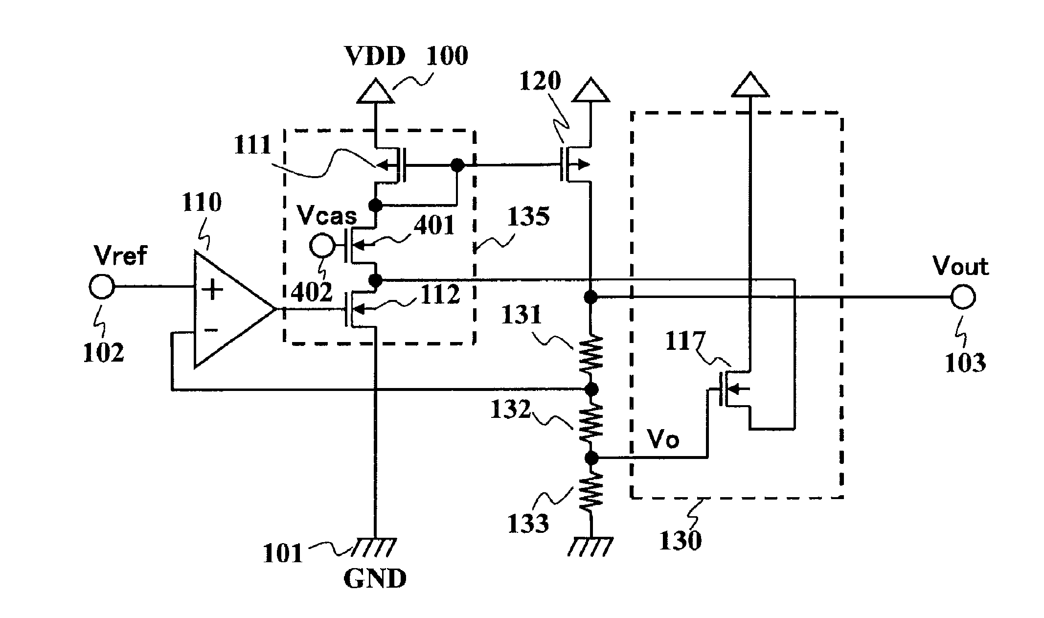
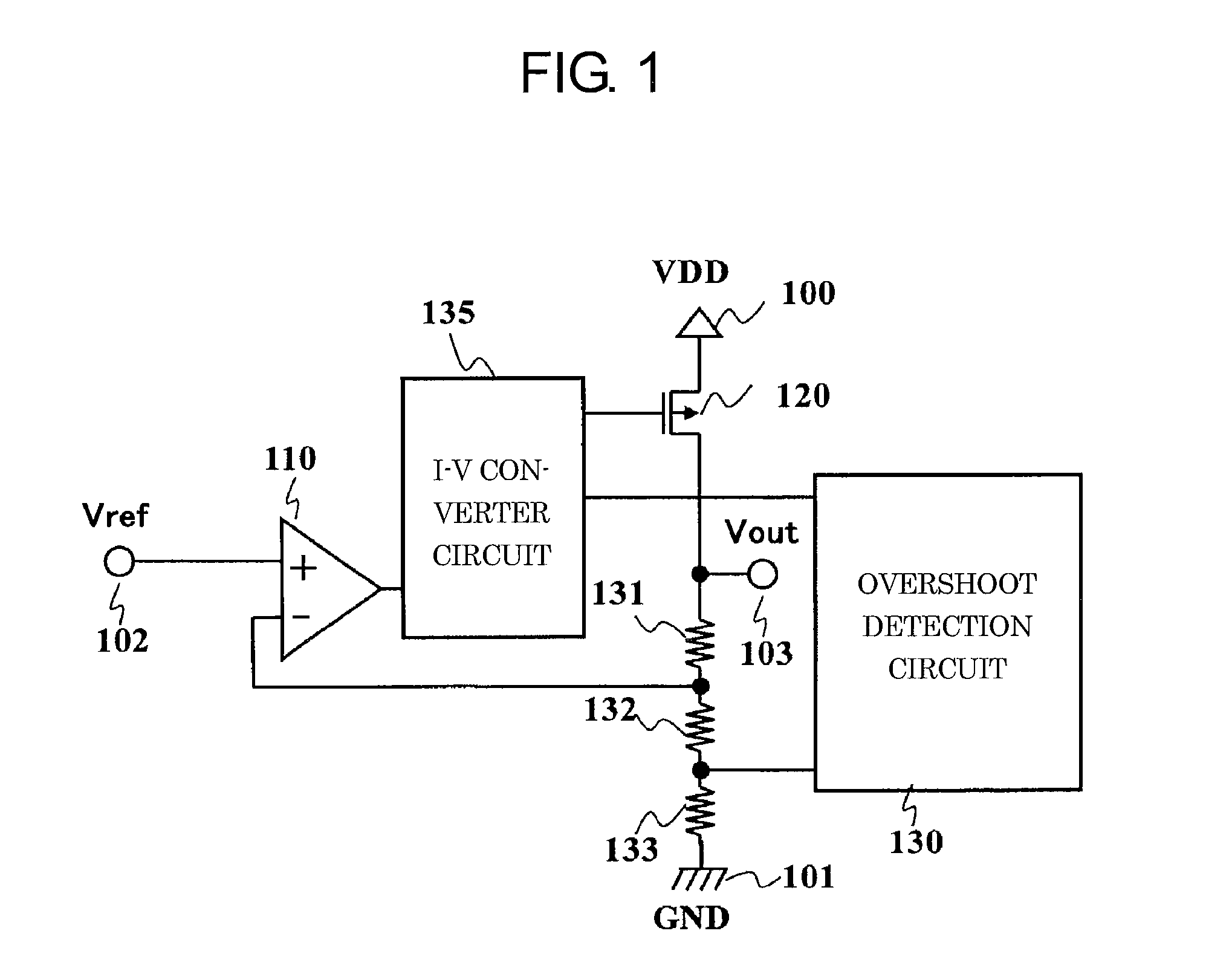
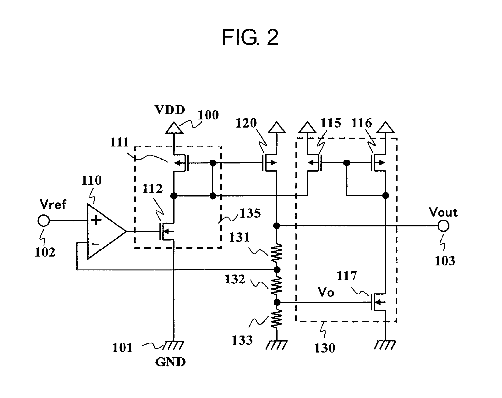
[0017]FIG. 1 is a block diagram of a voltage regulator according to an embodiment of the present invention. The voltage regulator according to this embodiment includes an error amplifier 110, a PMOS transistor 120, resistors 131, 132, and 133, an overshoot detection circuit 130, an I-V converter circuit 135, a power supply terminal 100, a ground terminal 101, a reference voltage terminal 102, and an output terminal 103. The PMOS transistor 120 operates as an output transistor. FIG. 2 is a circuit diagram of the voltage regulator according to this embodiment. The overshoot detection circuit 130 includes PMOS transistors 115 and 116 and an NMOS transistor 117. The I-V converter circuit 135 includes a PMOS transistor 111 and an NMOS transistor 112.
[0018]Next, connections in the voltage regulator according to this embodiment are described. The error amplifier 110 has a non-inverting input terminal connected to the reference voltage terminal 102, an inverting input terminal connected to ...
PUM
 Abstract
Description
Claims
Application Information