Detector structure for imaging applications and related method of manufacture

a technology of image processing and detector structure, applied in the field can solve the problems of limited application of hybrid pixel detectors, inability to meet the needs of imaging applications, and inability to meet the requirements of imaging applications, etc., and achieves the effects of increasing the cost of processing

Inactive Publication Date: 2014-09-25
ADVACAM OY
View PDF5 Cites 20 Cited by
  • Summary
  • Abstract
  • Description
  • Claims
  • Application Information

AI Technical Summary

Benefits of technology

[0006]The objective is to at least alleviate the problem described hereinabove and to provide a hybrid detector solution feasible for use in applications requiring generally larger detection areas than a single hybrid detector is, in practical applications, capable of sensibly establishing.

Problems solved by technology

Nevertheless, the applicability of hybrid pixel detectors is often limited by their relatively modest detection area size, which may typically be of the order of 10 square centimeters or less due to various technical challenges in the manufacturing of larger detectors resulting in a commercially unacceptable yield, for example.
The resulting processed image is typically far from perfect and remains technically and / or financially unfeasible in many applications.

Method used


Image

  • Detector structure for imaging applications and related method of manufacture
  • Detector structure for imaging applications and related method of manufacture
  • Detector structure for imaging applications and related method of manufacture

Examples


Embodiment Construction

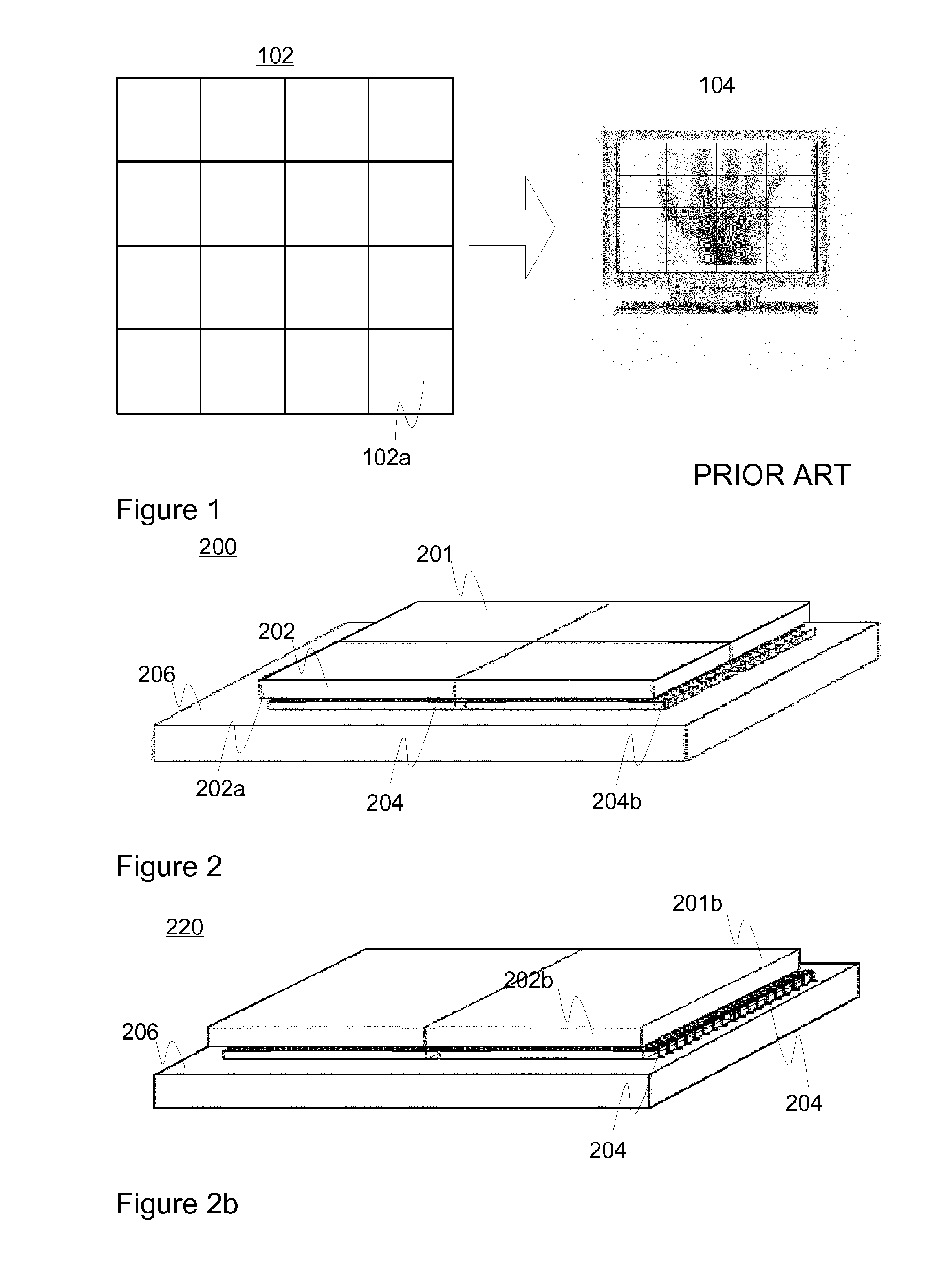
[0041]FIG. 1 was already reviewed in the background portion hereinbefore.

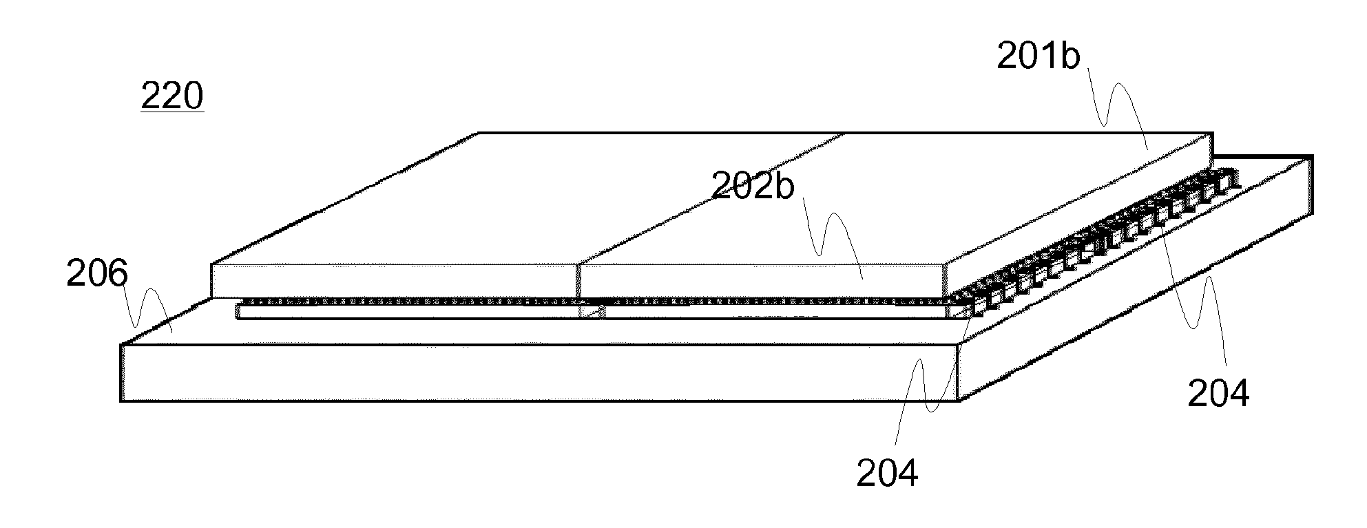
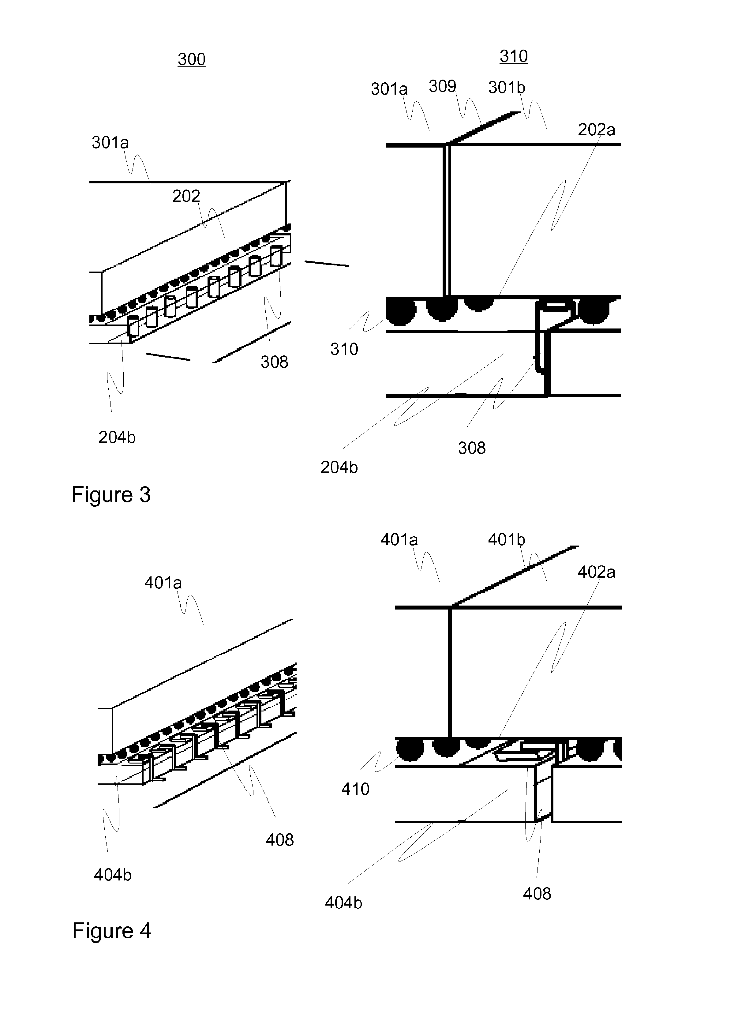
[0042]FIG. 2 illustrates an embodiment of the direct imaging hybrid pixel detector structure 200 in accordance with the present invention. In the figure, four detector entities, e.g. detector modules, 201 having edgeless detectors volumes 202 with self-supporting overhang portions 202a are shown as located adjacent to each other. In practice, the number of detector entities 201 combined as suggested herein may be considerably larger. For instance, an array of a desired number of detector entities such as 4×4, 8×8, 13×13, or 16×16 detector element arrays could be created. One detector entity may have a radiation sensitive surface of e.g. 1.4×1.4 cm̂2. The associated pixel size may be about 55 micrometers×55 micrometers, for instance. Each pixel may be connected to a read-out cell of the corresponding read-out element 204 that may process the charge signal by shaping and / or amplifying, count signals exceeding a d...


PUM


Abstract

A hybrid pixel detector structure including a plurality of detector entities, each detector entity including at least one read-out element, such as a read-out ASIC, and an overlapping substantially edgeless radiation sensitive detector volume, these two being electrically coupled utilizing a number of conductive elements in between, further including a substrate, such as a circuit board, or multiple substrates such as one per detector entity, for accommodating the plurality of detector entities, wherein the substantially edgeless detector volume of at least one detector entity of the plurality includes an overhang portion outside the overlap between the detector volume and the read-out element, and the read-out element of at least one other detector entity of the plurality includes an extension portion, also outside the overlap, with a number of electrical coupling elements to electrically couple to the substrate, such as conductors and/or electronics thereof. A corresponding method of manufacture is presented.

Description

FIELD OF THE INVENTION[0001]Generally the present invention pertains to radiation detectors. In particular, the present invention concerns hybrid pixel detectors.BACKGROUND[0002]Generally, hybrid pixel detector entities comprising detector material and a bump-bonded read-out integrated circuit (ROIC or just ROC) may be utilized for almost a myriad of purposes in the field of radiation imaging and are capable of providing quality-wise superior images. Accordingly, the hybrid detectors have many advantageous features such as high dynamic range, low noise, energy-sensitivity, etc. in contrast to most common alternative, basically indirect, imaging technologies like flat-panel technology suffering from noise, poorer contrast, blurring and inadequate dynamic range, or e.g. scintillation screens supplemented with (CCD) cameras also having poorer contrast and other flaws.[0003]Nevertheless, the applicability of hybrid pixel detectors is often limited by their relatively modest detection ar...

Claims


Application Information

Patent Timeline
Patent Type & Authority Applications(United States)
IPC IPC(8): H01L27/146
CPCH01L27/14661H01L27/14636H01L27/1467H01L2224/16225H01L27/1469H01L27/14601H10K19/901
Inventor KALLIOPUSKA, JUHAJAKUBEK, JAN
Owner ADVACAM OY
Why Eureka
Try Eureka