

Display device and electrical apparatus
- Summary
- Abstract
- Description
- Claims
- Application Information
AI Technical Summary
Benefits of technology
Problems solved by technology
Method used
Image

Examples
example 1
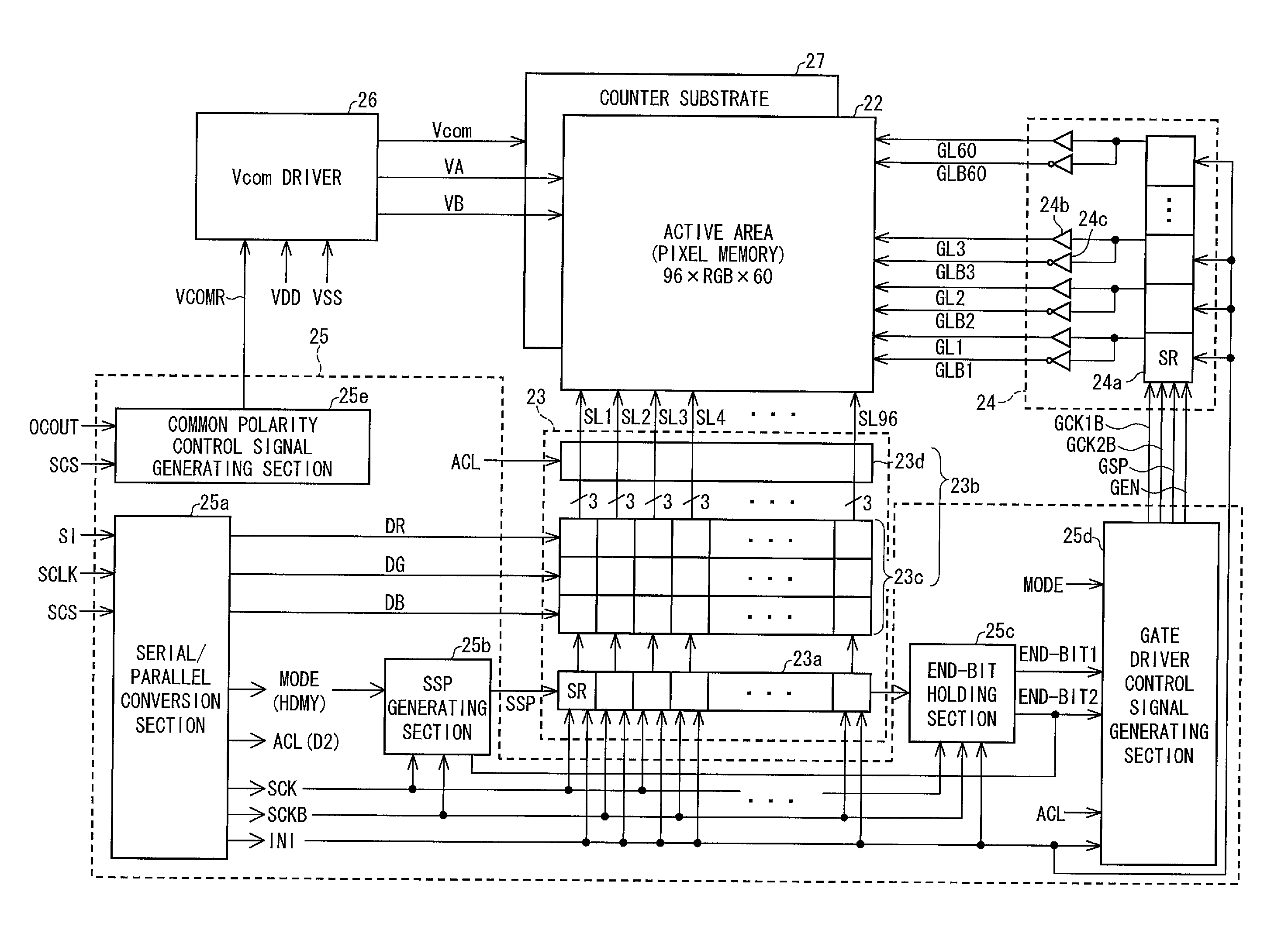
[0103]The following description will discuss a specific configuration of a common polarity control signal generating section 25e.
[0104]FIG. 14 is a circuit diagram illustrating a configuration of a common polarity control signal generating section 25e of Example 1. FIG. 15 is a timing chart illustrating signals which are received from and supplied to the common polarity control signal generating section 25e. The common polarity control signal generating section 25e includes a D flipflop 251e and a latch circuit 252e. FIG. 16 illustrates a circuit configuration of a D flipflop 251e. FIG. 17 illustrates a circuit configuration of a latch circuit 252e.
[0105]As illustrated in FIG. 16, the D flipflop 251e is constituted by clocked inverter circuits and inverter circuits. An input D1 is latched in synchronization with a rising edge of CK1, so that an output corresponding to the input D1 is supplied from an output terminal Q1 and an output terminal QB1.
[0106]The output QB1 of the D flipf...
example 2
[0121]The following description will specifically discuss a configuration of a common polarity control section 25f of Example 2.
[0122]In a case where a panel resolution is small, data rewriting time is short (see FIG. 18). This causes a time period, in which an SCS signal is in a high level (an active period), to be shorter than a cycle on which a common reverse needs to be carried out. As such, as with Example 1, the above effects can be brought about by controlling a common reverse timing in response to the SCS signal.
[0123]In contrast, in a case where the panel resolution is large, a data rewriting time is long (see FIG. 19). This causes a time period, in which the serial chip select signal SCS is in a high level (an active period), to be longer than a cycle on which a common reverse needs to be carried out. This causes a problem that with the configuration of Example 1, the common reverse is not properly carried out (see (a) of FIG. 19).
[0124]In order to address such a problem, ...
example 3
[0135]The following description will discuss a specific configuration of a common polarity control section 25g of Example 3.
[0136]The common polarity control section 25g of Example 3 is configured such that a timing signal which indicates a horizontal retrace period of the common polarity control section 25f of Example 2 is generated by a CPU 21d and is supplied to the common polarity control section 25g.
[0137]FIG. 22 is a circuit diagram illustrating a configuration of a common polarity control section 25g of Example 3. FIG. 23 is a timing chart illustrating signals which are received from and supplied to the common polarity control section 25g. The common polarity control section 25g includes a D flipflop 251g and a latch circuit 252g. The D flipflop 251g and the latch circuit 252g are identical in circuit configuration to the D flipflop 251e (FIG. 16) of Example 1 and the latch circuit 252e (FIG. 17) of Example 1, respectively. Moreover, the common polarity control section 25g i...
PUM
 Abstract
Description
Claims
Application Information