Low Power Management of Multiple Sensor Chip Architecture

a technology of multiple sensor and chip, applied in the field of multi- and varied communication sensors, can solve the problems of power consumption and limited device capability

Active Publication Date: 2014-11-27
GOOGLE TECH HLDG LLC
View PDF2 Cites 20 Cited by
  • Summary
  • Abstract
  • Description
  • Claims
  • Application Information

AI Technical Summary

Problems solved by technology

Furthermore, computing devices are typically battery operated and, as such, power consumption is an important feature in marketing these devi

Method used


Image

  • Low Power Management of Multiple Sensor Chip Architecture
  • Low Power Management of Multiple Sensor Chip Architecture
  • Low Power Management of Multiple Sensor Chip Architecture

Examples


Embodiment Construction

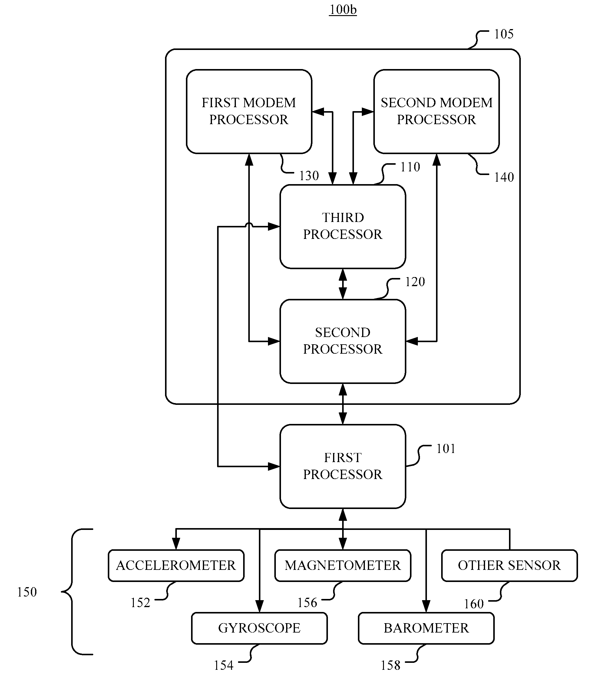
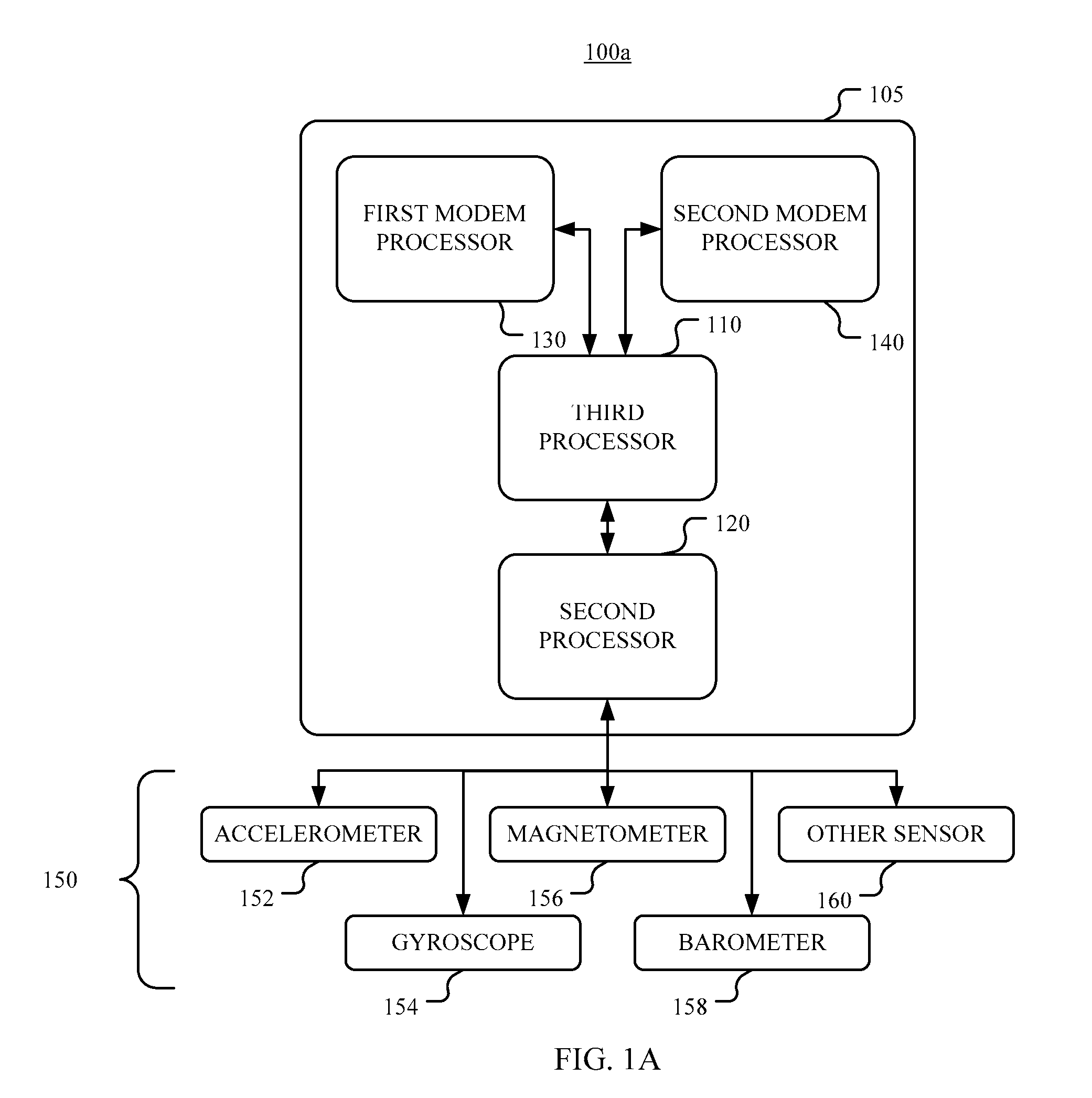
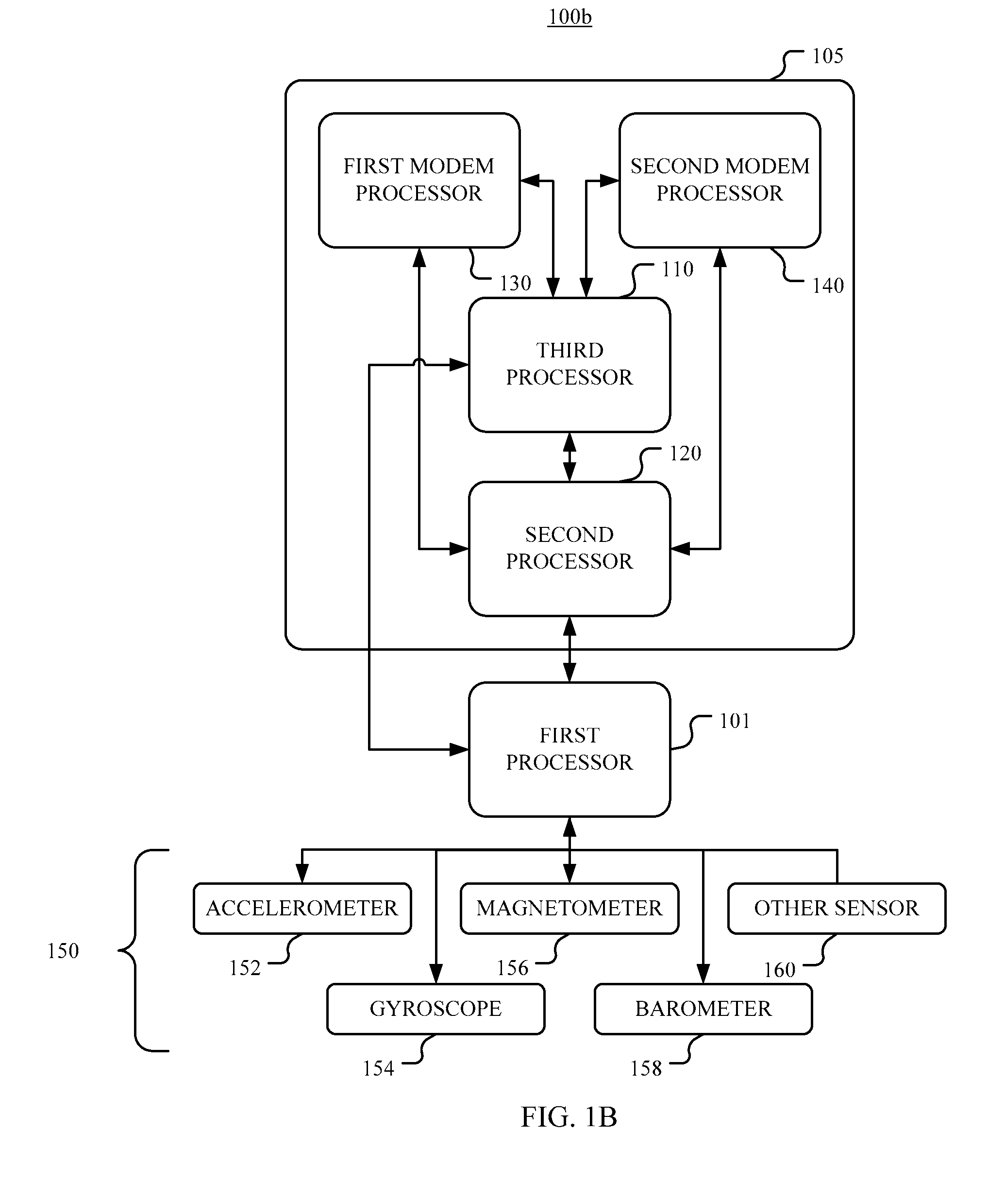
[0027]Described herein is a method for managing processor analysis of multiple sensors in a computing device that includes monitoring a first sensor signal that may be coupled to a sensor hub processor and thereafter comparing the first monitored sensor signal with a predetermined signature for establishing a confidence relationship associated with received sensor signaling from multiple sensors. Alternatively, the first monitored sensor signal may simply be compared with the predetermined signature.

[0028]In addition, the efficacy of operation for the multiple sensors may be determined; and a second sensor signal that is coupled to a low power core may be monitored. The second monitored sensor signal may be compared with another predetermined signature for establishing a confidence relationship associated with received sensor signaling from multiple sensors. The method confirms that one or more sensors has met a predetermined confidence state.

[0029]In one embodiment, a short range w...


PUM


Abstract

A method, device, system, or article of manufacture is provided for low-power management of multiple sensor chip architecture. In one embodiment, a method comprises, at a computing device that includes a first processor, a second processor and a third processor, receiving, at the first processor, first sensor data from a first sensor; determining, at the first processor, a motion state of the computing device using the first sensor data; in response to determining that the motion state corresponds to a predetermined motion state, activating the second processor; receiving, at the second processor, second sensor data from a second sensor; determining, by the second processor, that the motion state corresponds to the predetermined motion state using the second sensor data; and, in response to determining that the motion state corresponds to the predetermined motion state using the second sensor data, sending the motion state to the third processor.

Description

CROSS-REFERENCE TO RELATED APPLICATIONS[0001]This application claims priority to U.S. Provisional Patent Application No. 61 / 728,921, filed Nov. 21, 2012, entitled “LOW POWER MANAGEMENT OF MULTIPLE SENSOR CHIP ARCHITECTURE,” U.S. Provisional Patent Application No. 61 / 776,868, filed Mar. 12, 2013, entitled “LOW POWER MANAGEMENT OF MULTIPLE SENSOR CHIP ARCHITECTURE,” and U.S. Provisional Patent Application No. 61 / 827,458, filed May 24, 2103, entitled “LOW POWER MANAGEMENT OF MULTIPLE SENSOR CHIP ARCHITECTURE,” all of which the contents are hereby incorporated by reference as if fully set forth below.FIELD OF USE[0002]The embodiments described herein relate to multiple and varied communication sensors within an integrated chip architecture and more particularly to managing sensor data from the multiple and varied communication sensors.BACKGROUND[0003]In today's sophisticated computing devices such as mobile computing devices, smartphones, tablet computers, and wearable computing devices...

Claims


Application Information

Patent Timeline
IPC IPC(8): G06F15/80
CPCG06F15/80G06F1/3206G06F3/0346H04W52/0251Y02D30/70G06F1/324G06F1/3293
Inventor LAUTNER, DOUGLAS ADEBATES, SCOTT PHOR-LAO, MARY KFOREST, FRANCIS WSHAH, JAGATKUMAR V
Owner GOOGLE TECH HLDG LLC
Why Eureka
Try Eureka