Method for Temporary Electrical Contacting of a Component Arrangement and Apparatus Therefor

a technology of component arrangement and electrical contact, which is applied in the direction of fault location by increasing the damage at fault, individual semiconductor device testing, instruments, etc., can solve the problems of limited space between surfaces which may be contacted simultaneously, comparatively high process cost, and negative impact, so as to achieve reliable and inexpensive electrical contact the effect of the number of connections

Inactive Publication Date: 2014-12-04
OSRAM OPTO SEMICONDUCTORS GMBH
View PDF5 Cites 2 Cited by
  • Summary
  • Abstract
  • Description
  • Claims
  • Application Information

AI Technical Summary

Benefits of technology

[0004]Embodiments of the invention provide a method of electrical contacting, with which a large number of electrical connections may be produced reliably and inexpensively. Furthermore, an apparatus is to be provided which makes possible reliable electrical contacting.

Problems solved by technology

These processes, however, are comparatively expensive, which has a negative impact especially in the case of processes in which a large number of electrical contacts are to be made simultaneously.
Furthermore, in particular, when using spring contact pins, the space between surfaces which may be contacted simultaneously is limited.

Method used


Image

  • Method for Temporary Electrical Contacting of a Component Arrangement and Apparatus Therefor
  • Method for Temporary Electrical Contacting of a Component Arrangement and Apparatus Therefor
  • Method for Temporary Electrical Contacting of a Component Arrangement and Apparatus Therefor

Examples


Embodiment Construction

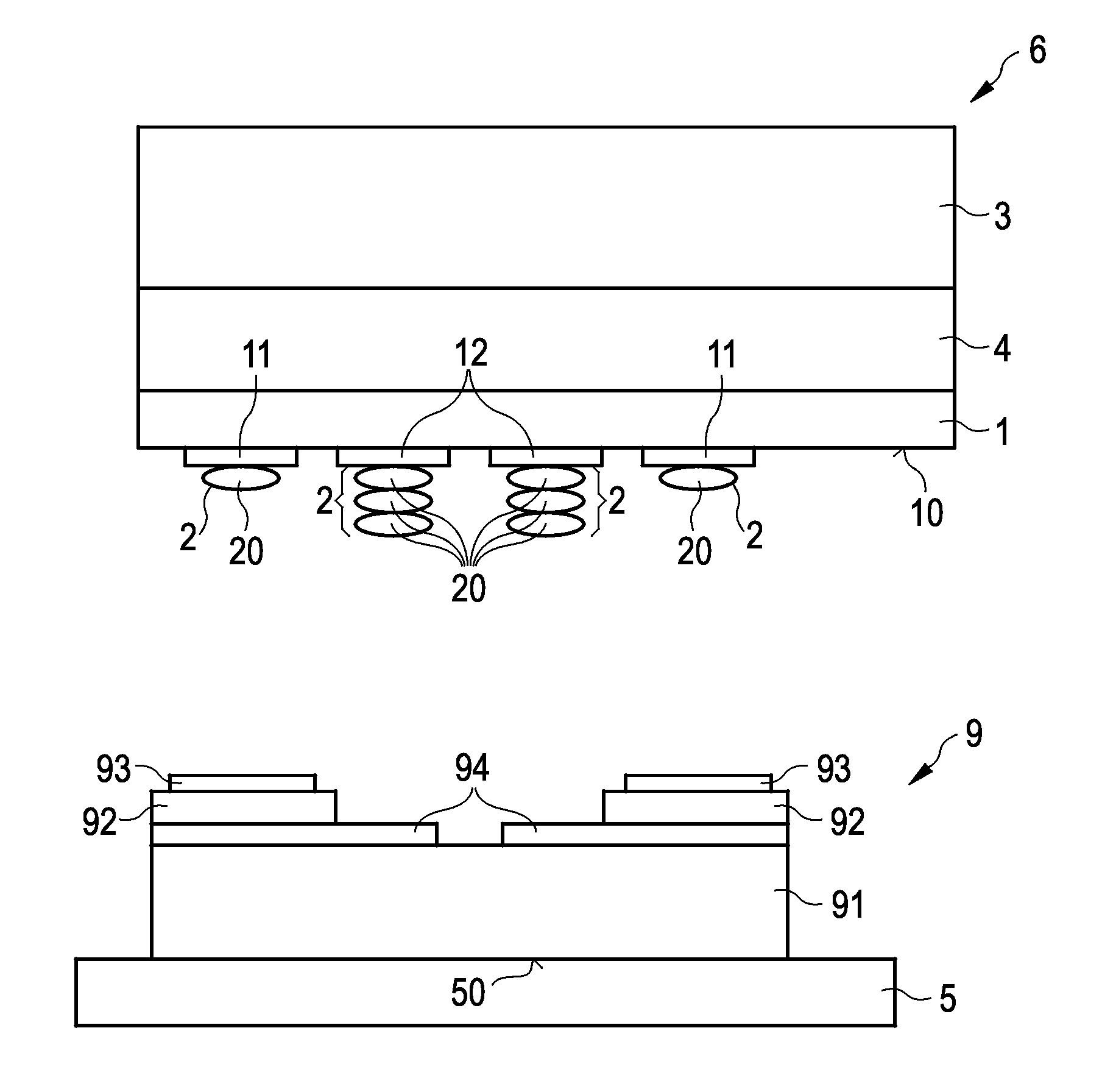
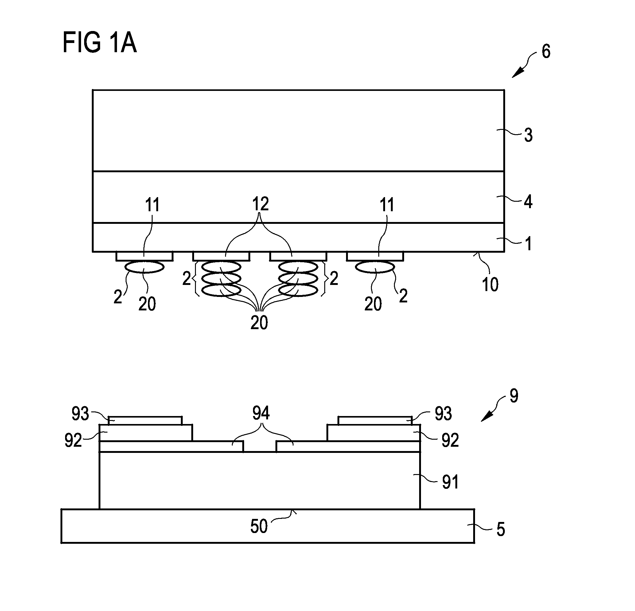
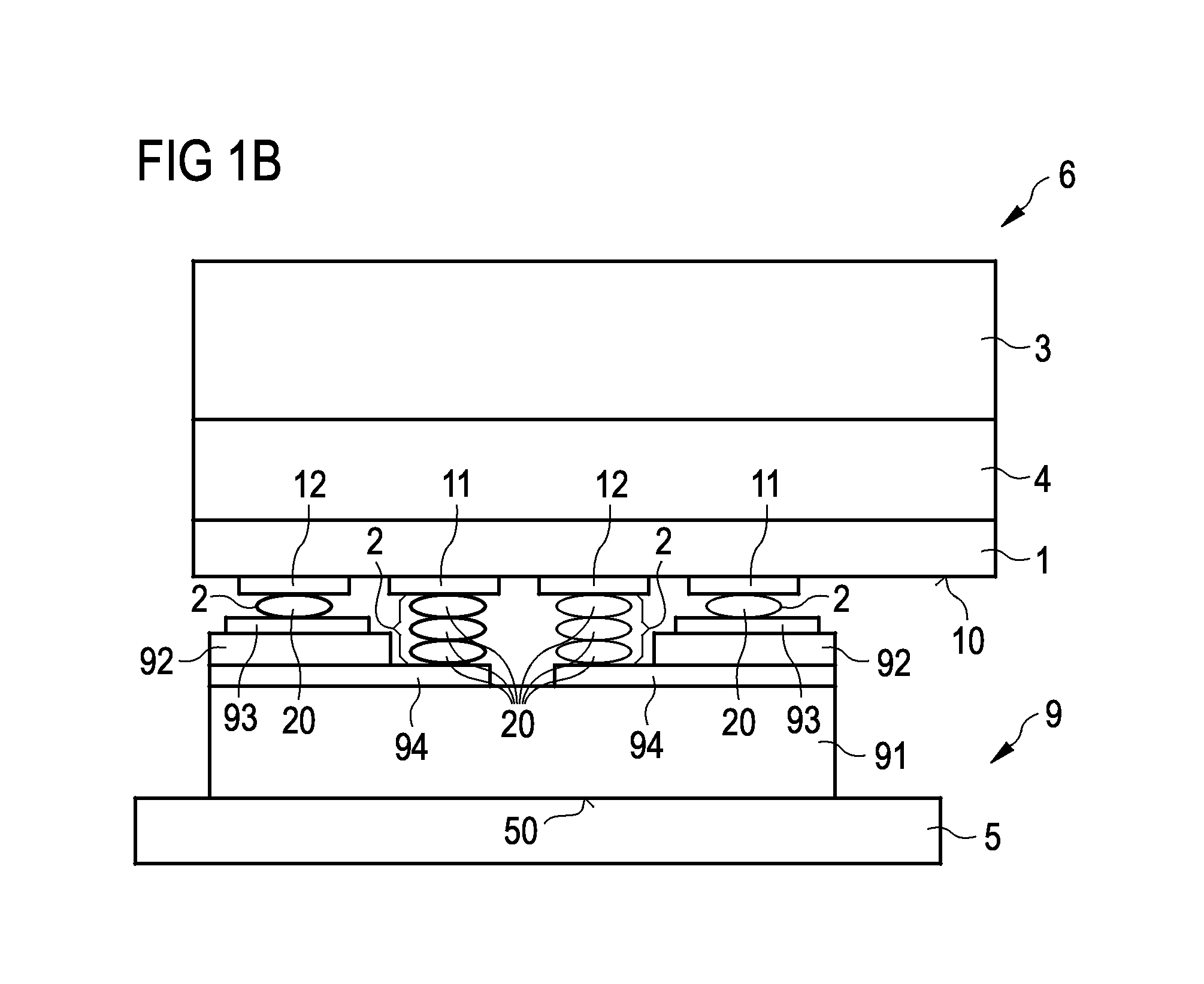
[0037]In FIG. 1A a schematic cross-sectional view of an exemplary embodiment for an apparatus 6 is shown. The method is described merely by way of example with the aid of a component arrangement 9 in which two components 92 are disposed next to each other. The components 92 are each electrically contactable by means of a first contact surface 93 and a second contact surface 94. The components 92 may be designed as semiconductor components, in particular as optoelectronic semiconductor components, for example, as luminescence diodes, such as semiconductor lasers.

[0038]In the illustrated exemplary embodiment the components 92 are disposed on an intermediate support 91. This intermediate support may be divided, after the temporary electrical contacting, for separation of the component arrangement into a plurality of components. As a deviation therefrom, the components may also be provided already singulated.

[0039]The first contact surface 93 and the second contact surface 94 are spaced...


PUM


Abstract

A method for temporary electrical contacting of a component arrangement with a plurality of contact surfaces is described. A connection support includes a plurality of connection surfaces, on which contact protrusions are disposed. The connection support and component arrangement are brought together in such a way that the connection surfaces and the associated contact surfaces overlap in a top view and the contact protrusions form an electrical contact with respect to the contact surfaces in order to achieve electrical contacting of the component arrangement. Subsequently the connection support and the component arrangement are separated from each other.

Description

[0001]This patent application is a national phase filing under section 371 of PCT / EP2012 / 067806, filed Sep. 12, 2012, which claims the priority of German patent application 10 2011 113 430.5, filed Sep. 14, 2011, each of which is incorporated herein by reference in its entirety.TECHNICAL FIELD[0002]The present patent application relates to a method for electrical contacting of a component arrangement and an apparatus for carrying out the method.BACKGROUND[0003]Electronic or optoelectronic components are often temporarily contacted in order to carry out test or burn-in processes. For this purpose it is possible to use, for example, probe cards, arrangements of spring contact pins or test bases with spring contact pins. These processes, however, are comparatively expensive, which has a negative impact especially in the case of processes in which a large number of electrical contacts are to be made simultaneously. Furthermore, in particular, when using spring contact pins, the space be...

Claims


Application Information

Patent Timeline
Patent Type & Authority Applications(United States)
IPC IPC(8): G01R1/067G01R31/28
CPCG01R31/2855G01R1/067G01R1/06744G01R1/07321G01R1/0735G01R31/2635
Inventor KUEHNELT, MICHAELENZMANN, ROLAND
Owner OSRAM OPTO SEMICONDUCTORS GMBH
Why Eureka
Try Eureka