Compact Level Shifter

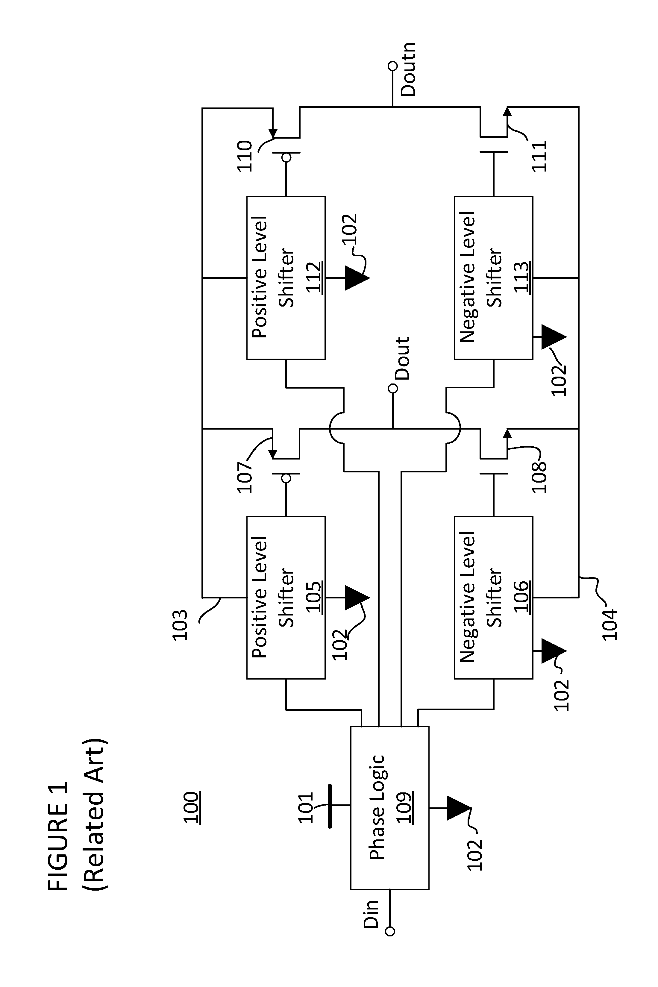
a level shifter and compact technology, applied in the direction of logic circuit coupling/interface arrangement, pulse automatic control, pulse technique, etc., can solve the problem that the phasing of complementary signals is not suitable for controlling the additional set of output buffer devices, the power available at those voltage levels is somewhat limited, and the inability to generate doutn at node dout is not sufficient for most applications

Active Publication Date: 2014-12-04
QUALCOMM INC
View PDF3 Cites 14 Cited by
  • Summary
  • Abstract
  • Description
  • Claims
  • Application Information

AI Technical Summary

Benefits of technology

[0017]In specific embodiments of the present invention, a device for level shifting an input signal is provided. The device includes an output buffer that has: an output node, a p-FET coupled to a high reference voltage, and an n-FET coupled to a low reference voltage. The device also includes two latches. The first latch has a first latch output that drives a gate of the p-FET via an inverting circuit element. The second latch has a second latch output that drives a gate of the n-FET via a non-inverting circuit element. The device also includes a reset signal pulse generator that receives the input signal and generates a reset signal pulse in response to a transition in the input signal. Both of the latches are placed in a reset state by the reset signal pulse.
[0018]In other embodiments of the present invention a pr

Problems solved by technology

Furthermore, the high and low supply voltages 103 and 104 are, in the context of an integrated circuit, usually generated on chip using a pump circuit so that the amount of power available at those voltages levels is somewhat limited.
Placing an inverter at node Dout to generate Doutn is not sufficient for most applications be

Method used


Image

  • Compact Level Shifter
  • Compact Level Shifter
  • Compact Level Shifter

Examples


Embodiment Construction

[0020]Reference now will be made in detail to embodiments of the disclosed invention, one or more examples of which are illustrated in the accompanying drawings. Each example is provided by way of explanation of the present technology, not as a limitation of the present technology. In fact, it will be apparent to those skilled in the art that modifications and variations can be made in the present technology without departing from the spirit and scope thereof. For instance, features illustrated or described as part of one embodiment may be used with another embodiment to yield a still further embodiment. Thus, it is intended that the present subject matter covers all such modifications and variations within the scope of the appended claims and their equivalents.

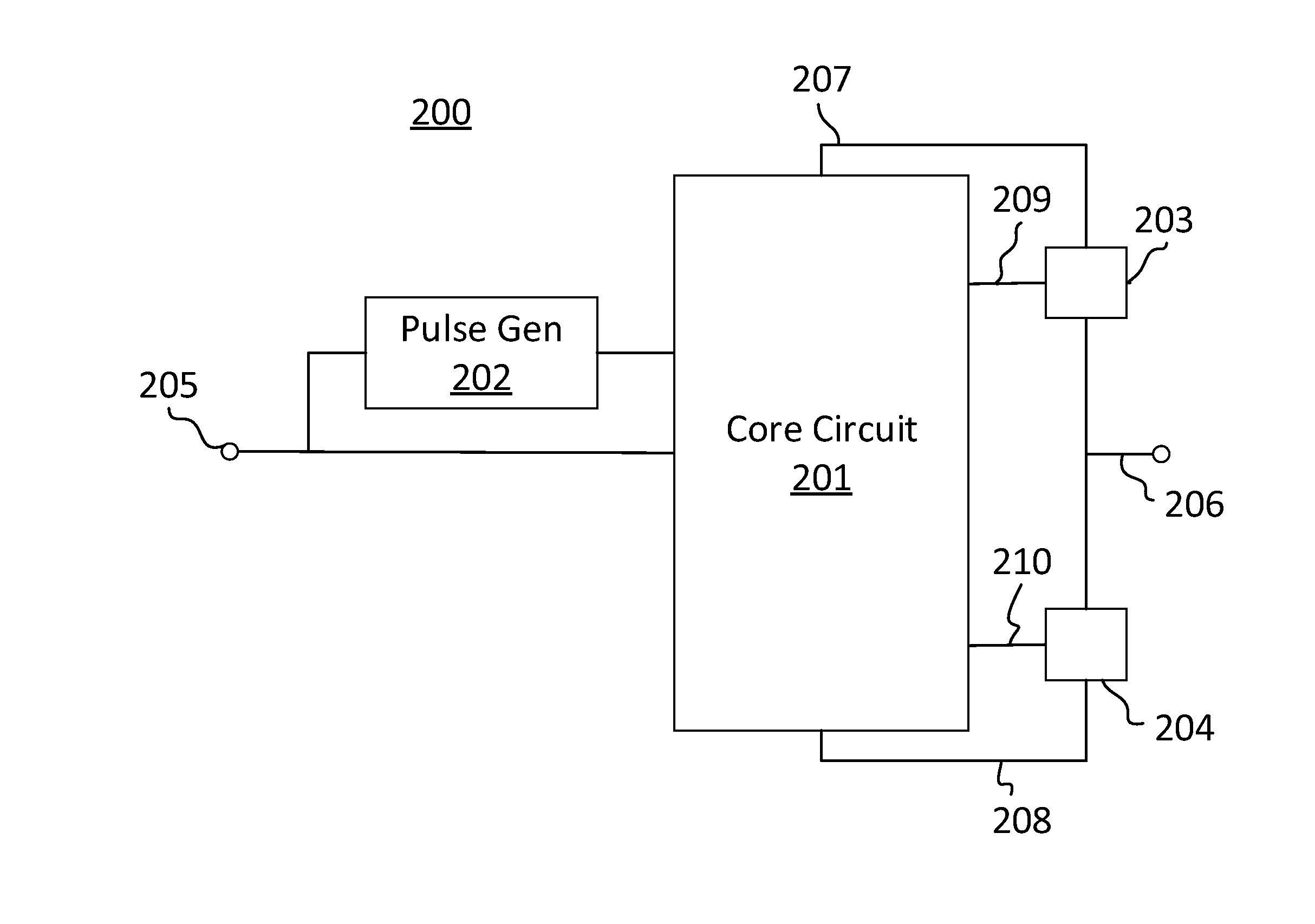
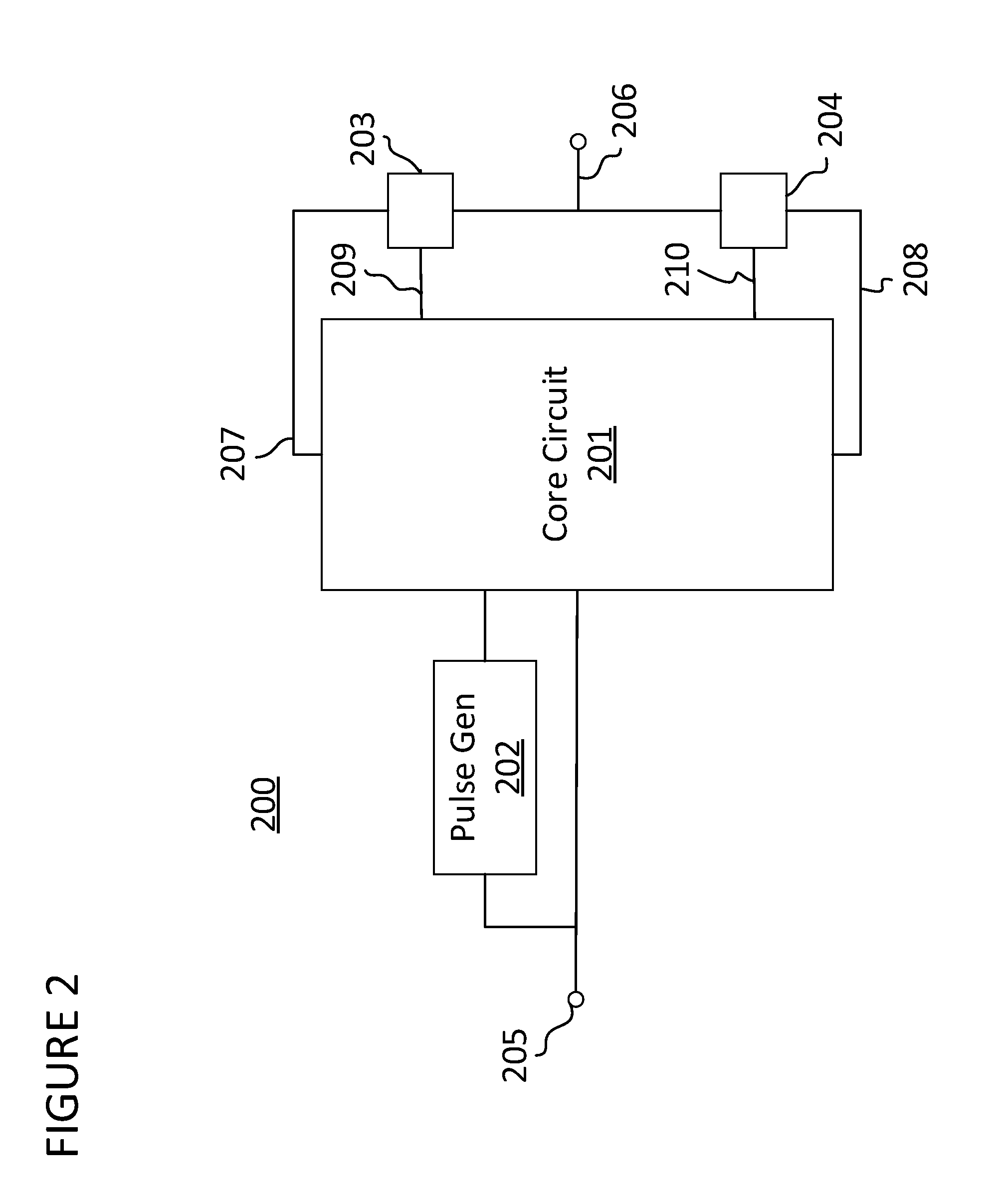
[0021]The present disclosure relates to electronic circuits. In particular, the present disclosure relates to electronic circuits with output signals having larger magnitudes than their input signals. In the following descrip...


PUM


Abstract

Embodiments of the present invention provide a device for level shifting an input signal. The device includes an output buffer that has: an output node, a p-FET coupled to a high reference voltage, and an n-FET coupled to a low reference voltage. The device also includes two latches. The first latch has a first latch output that drives a gate of the p-FET via an inverting circuit element. The second latch has a second latch output that drives a gate of the n-FET via a non-inverting circuit element. The device also includes a reset signal pulse generator that receives the input signal and generates a reset signal pulse in response to a transition in the input signal. Both of the latches are placed in a reset state by the reset signal pulse.

Description

BACKGROUND OF THE INVENTION[0001]A level shifter alters the magnitude of a signal. They are often utilized to convert digital signals operating in one domain to signals in a different domain. For example, a level shifter might take in an analog signal from a circuit operating with a supply voltage of 1 volt, and transfer the signal into a circuit operating with a supply voltage of 2 volts. In this example, each value of the signal in the 1 volt domain would be represented by a factor of two larger value of the signal in the 2 volt domain. As another example, a level shifter might take in a digital signal operating with a transistor-transistor logic level and convert the signal to different domain. Since digital signals are either logic high or logic low values, the transistor-transistor logic level digital signal would be level shifted to a create a new version of the signal with logic high and logic low values equivalent to the logic high and logic low values of the new domain.[000...

Claims


Application Information

Patent Timeline
IPC IPC(8): H03K19/0175
CPCH03K19/017509H03K3/356182
Inventor LOU, PERRY
Owner QUALCOMM INC
Why Eureka
Try Eureka