Thin film semiconductors made through low temperature process

a technology of thin film and low temperature, applied in the direction of semiconductor devices, basic electric elements, electrical appliances, etc., can solve the problem of limited tft performan

Active Publication Date: 2014-12-11
APPLIED MATERIALS INC
View PDF2 Cites 4 Cited by
  • Summary
  • Abstract
  • Description
  • Claims
  • Application Information

AI Technical Summary

Benefits of technology

This patent relates to ways to make a thin film transistor (TFT) that can operate at lower temperatures. One way this is done is by creating a layer made from nitrides or oxynitrides which are exposed to air or other gases containing moisture to change their properties. Another method involves putting the layers through physical treatment like dipping them in water or heating them with steam. These changes allow the material to better function when used in a TFT.

Problems solved by technology

The technical problem addressed in this patent text relates to improving the performance of thin-film transistors (TFTs) used in display screens. Current methods involve limiting the annealing and deposition temperatures due to limitations imposed by the substrate, resulting in poorer performance of the TFTs. There is thus a need for a new approach that can overcome this limitation and improve the quality and reliability of TFTs.

Method used


Image

  • Thin film semiconductors made through low temperature process
  • Thin film semiconductors made through low temperature process

Examples


Embodiment Construction

[0015]Embodiments disclosed herein relate to a TFT and methods for manufacture thereof. Specifically, the embodiments herein relate to methods for forming the semiconductor layer in a TFT at a low temperature. The semiconductor layer may be formed by depositing a nitride layer or oxynitride layer, such as zinc nitride or oxynitride, and then converting the layer into a layer with a different oxygen content than before. The conversion occurs by exposing the nitride or oxynitride layer to air with high relative humidity up to 100 degrees Celsius or steam or a gas with water vapor at a temperature above 100 degrees Celsius; physically dipping the nitride or oxynitride layer into water; or heating the substrate to a temperature of between about 100 degrees Celsius and about 200 degrees Celsius while exposing the nitride layer to steam.

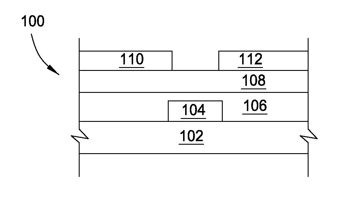
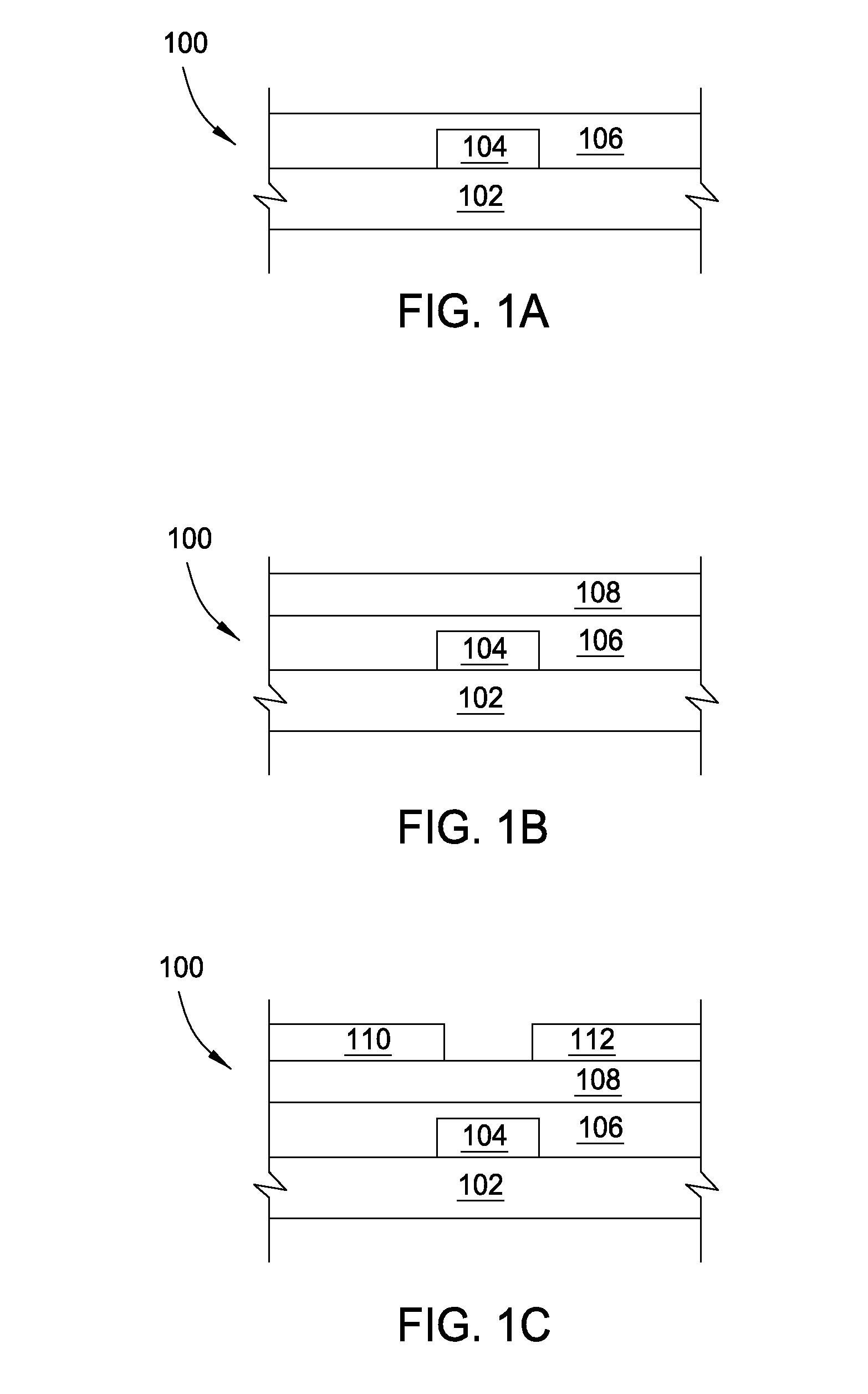
[0016]FIGS. 1A-1C are schematic cross-sectional views of a TFT 100 at various stages of production. As shown in FIG. 1A, a gate electrode 104 is formed ov...


PUM


Abstract

Embodiments disclosed herein relate to a TFT and methods for manufacture thereof. Specifically, the embodiments herein relate to methods for forming a semiconductor layer at a low temperature for use in a TFT. The semiconductor layer may be formed by depositing a nitride or oxynitride layer, such as zinc nitride or oxynitride, and then converting the nitride layer into an oxynitride layer with a different oxygen content. The oxynitride layer is formed by exposing the deposited nitride layer to a wet atmosphere at a temperature between about 85 degrees Celsius and about 150 degrees Celsius. The exposure temperature is lower than the typical deposition temperature used for forming the oxynitride layer directly or annealing, which may be performed at temperatures of about 400 degrees Celsius.

Description


Claims


Application Information

Patent Timeline
Owner APPLIED MATERIALS INC
Why Eureka
Try Eureka