
Zinc nitride compound and method for producing same

a technology of zinc nitride and compound, which is applied in the direction of luminescent composition, sustainable manufacturing/processing, final product manufacturing, etc., can solve the problems of unsuitable use in light-emitting devices or high-efficiency solar cells

Active Publication Date: 2018-12-13
PANASONIC CORP
View PDF0 Cites 1 Cited by
  • Summary
  • Abstract
  • Description
  • Claims
  • Application Information

AI Technical Summary

Benefits of technology

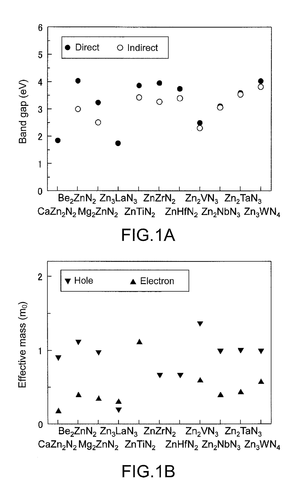
The invention provides a zinc nitride compound suitable for use in electronic devices such as high-speed transistors, efficient light-emitting devices, solar cells, and light sensors.

Problems solved by technology

However, GaN has a wide band gap and therefore cannot emit light in the visible range by itself.
Various zinc nitride compounds have been proposed; however, for example, ZnSnN2 is difficult to produce in the form of a p-type semiconductor, and Ca2ZnN2 is an indirect band gap semiconductor.
The problem with these zinc nitride compounds is that, for example, they are unsuitable for use in light-emitting devices or high-efficiency solar cells (Non Patent Literature 1).

Method used


Image

  • Zinc nitride compound and method for producing same
  • Zinc nitride compound and method for producing same
  • Zinc nitride compound and method for producing same

Examples


example 2

[0069]Synthesis of Zinc Nitride Compound Represented by CaZn2N2

[0070]Starting compounds, Ca3N2 and Zn3N2 mixed in a molar ratio Ca3N2:Zn3N2 of 1:2, were introduced into a high-pressure cell and subjected to high-pressure synthesis in which a pressure of 5.0 GPa was applied at 1200° C. for 1 hour. The high-pressure synthesis apparatus used is a belt-type high-pressure synthesis apparatus which has a high-pressure cell as a sample holder, whose pressure control range is from 2 to 5.5 GPa, and whose temperature control range is from room temperature to 1600° C.

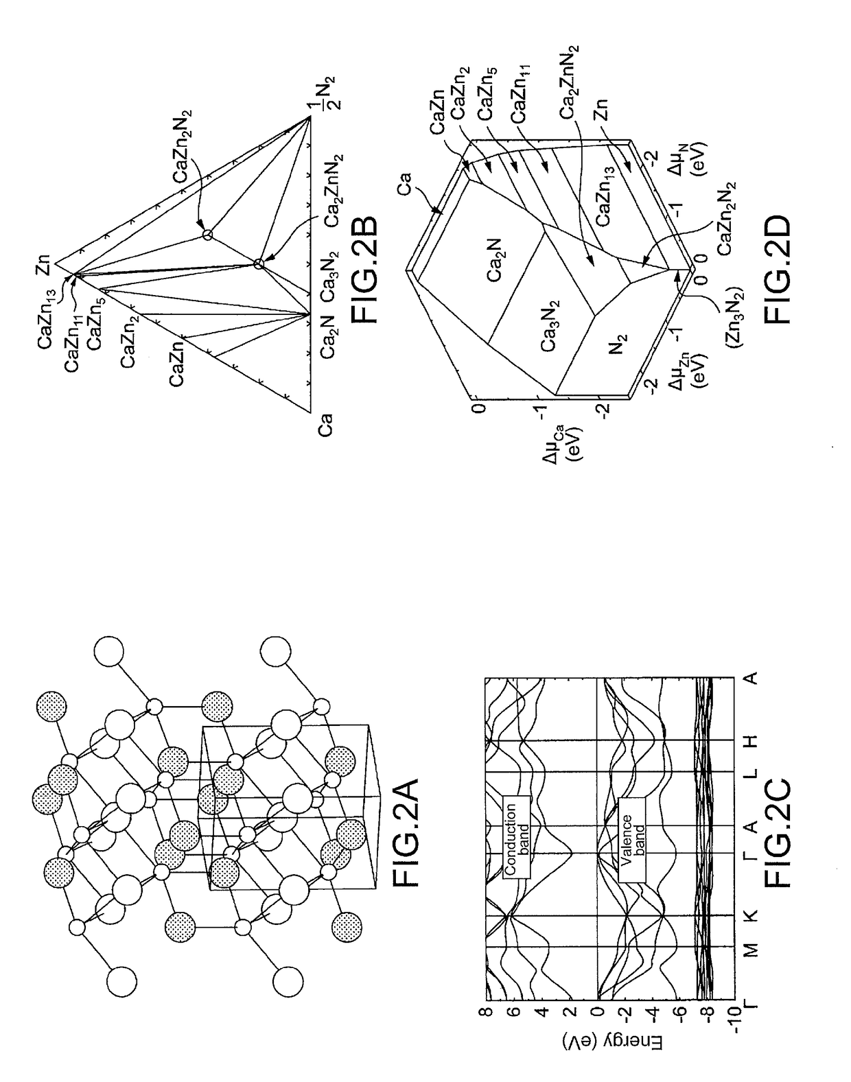
[0071]X-ray diffraction patterns of the resulting high-pressure synthesis product are shown in FIG. 8. About 80 wt % of the product consisted of CaZn2N2, and the rest consisted of Zn etc. As for the lattice parameters of CaZn2N2, the lattice parameters a and c were respectively 3.46380(11) Å and 6.00969(30) Å which differ by 0.3% from the theoretical lattice parameters a and c of 3.454 Å and 5.990 Å.

[0072]Light emission, in parti...


PUM

PropertyMeasurementUnit
band gapaaaaaaaaaa
pressureaaaaaaaaaa
band gapaaaaaaaaaa

Abstract

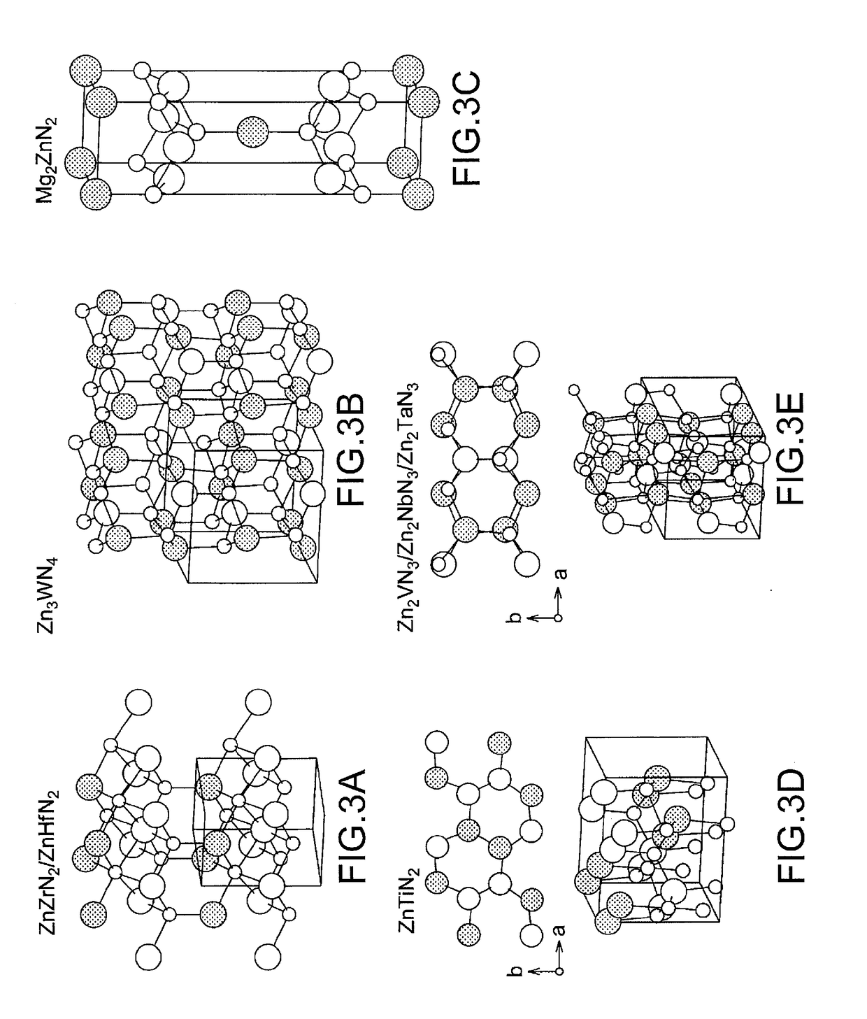
The present invention provides a zinc nitride compound suitable for electronic devices such as high-speed transistors, high-efficiency visible light-emitting devices, high-efficiency solar cells, and high-sensitivity visible light sensors. The zinc nitride compound is represented, for example, by the chemical formula CaZn2N2 or the chemical formula X12ZnN2 wherein X1 is Be or Mg. The zinc nitride compound is preferably synthesized at a high pressure of 1 GPa or more.

Description

TECHNICAL FIELD[0001]The present invention relates to a zinc nitride compound and a method for producing the same.BACKGROUND ART[0002]GaN is widely used in LED light sources. However, GaN has a wide band gap and therefore cannot emit light in the visible range by itself. InN has too narrow a band gap, due to which it cannot emit light in the visible range. Ga is a high-cost element, and In is a scarce element. Various zinc nitride compounds have been proposed; however, for example, ZnSnN2 is difficult to produce in the form of a p-type semiconductor, and Ca2ZnN2 is an indirect band gap semiconductor. The problem with these zinc nitride compounds is that, for example, they are unsuitable for use in light-emitting devices or high-efficiency solar cells (Non Patent Literature 1).CITATION LISTNon Patent Literature[0003]Non Patent Literature 1: J. Solid State Chem. 88, 528-533 (1990)SUMMARY OF INVENTIONTechnical Problem[0004]It is an object of the present invention to solve the above pro...

Claims


Application Information

Patent Timeline
Patent Type & Authority Applications(United States)
IPC IPC(8): C01B21/06C09K11/08C09K11/55H01L29/24H01L33/26H01L31/032
CPCC01B21/0602C09K11/0883C09K11/55H01L29/24H01L33/26H01L31/032C01P2006/40C01P2002/77C01P2002/72C09K11/54H01L31/18C01G9/00C01G9/006C01G9/08H01L31/0248H01L31/0256H01L33/00Y02P70/50
Inventor OBA, FUMIYASUHOSONO, HIDEOHIRAMATSU, HIDENORIKUMOMI, HIDEYAKUMAGAI, YUIIMURA, SOSHIMURABA, YOSHINORIBURTON, LEE ALANTANAKA, ISAOHINUMA, YOYO
Owner PANASONIC CORP
Learn More