
Method for pixel arrangement and display pannel using the same

a technology of pixel arrangement and display pannel, which is applied in the direction of thermoelectric device junction materials, electrical equipment, semiconductor devices, etc., can solve the problems of color cast problem, difficult to increase the resolution ratio of the image (ppi) displayed by the oled display screen, and reduce the yield of products, so as to reduce the area occupied by the sub-pixels, increase the physical resolution, and the effect of increasing the nts

Inactive Publication Date: 2015-01-15
EVERDISPLAY OPTRONICS (SHANGHAI) CO LTD
View PDF1 Cites 10 Cited by
  • Summary
  • Abstract
  • Description
  • Claims
  • Application Information

AI Technical Summary

Benefits of technology

The present disclosure provides a method for arranging pixels that reduces the space taken up by sub-pixels, increases the physical resolution, achieves better image quality in NTSC format, and reduces power dissipation in the display.

Problems solved by technology

However, due to the limitation of the manufacturing art of OLED, the resolution ratio of the image (PPI) displayed by OLED display screens is hard to increase, which becomes the choke point in the OLED development.
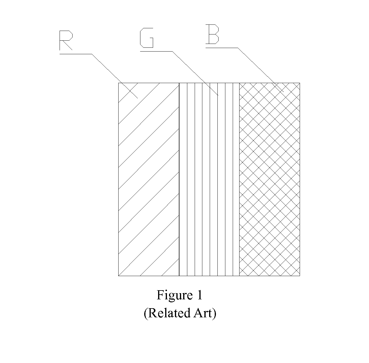
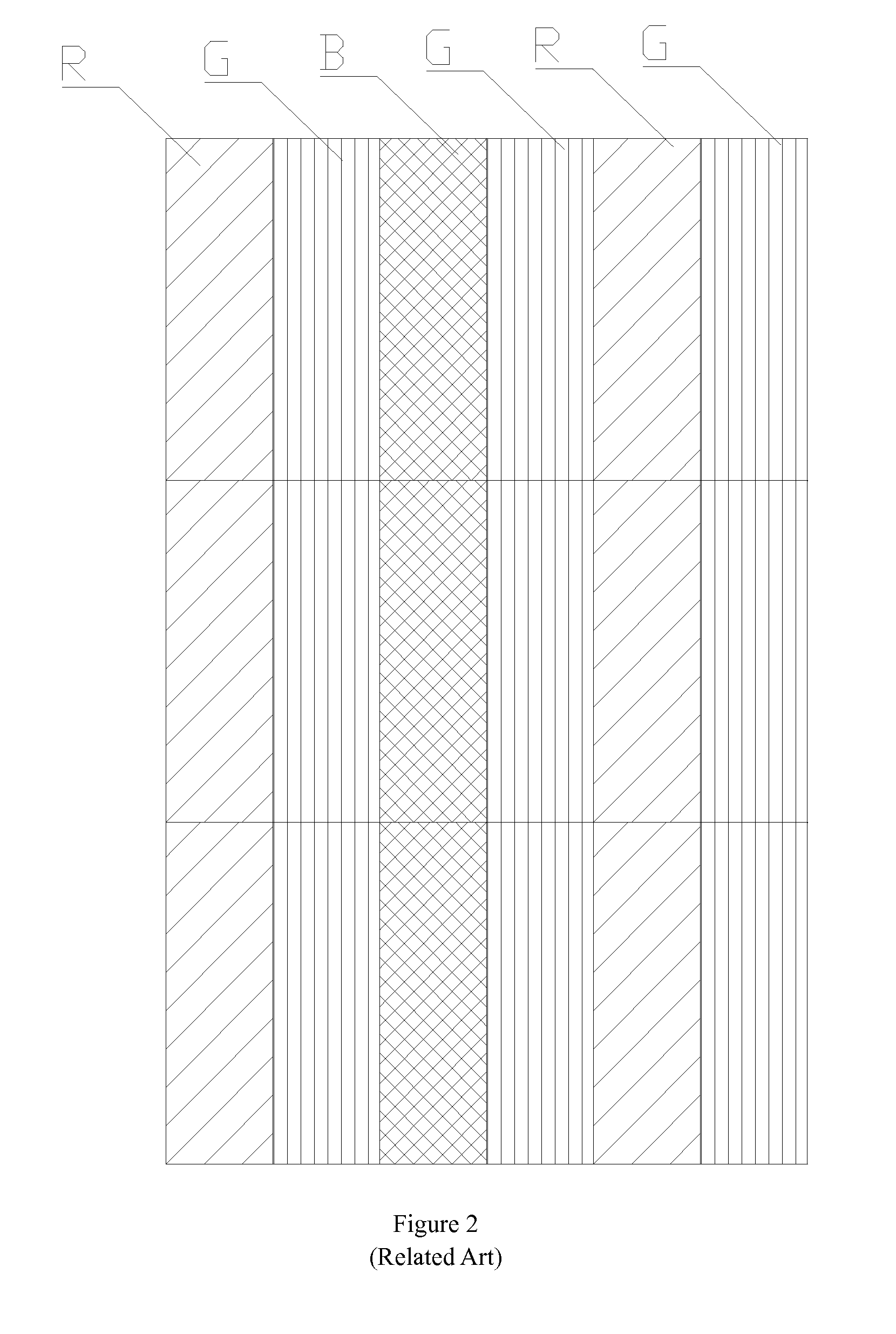
However, such pixel arrangement applied to OLED may cause the color mixture problem in the vapor deposition process, which will decrease the yield of products.
Therefore, it is easy to cause the color cast problem, which is not of benefit to the performance of OLED.

Method used


Image

  • Method for pixel arrangement and display pannel using the same
  • Method for pixel arrangement and display pannel using the same
  • Method for pixel arrangement and display pannel using the same

Examples


Embodiment Construction

[0052]The present invention will now be described more fully hereinafter with reference to the accompanying drawings, in which exemplary embodiments of the invention are shown. This invention may, however, be embodied in many different forms and should not be construed as limited to the embodiments set forth herein. Rather, these embodiments are provided so that this disclosure will be thorough and complete, and will fully convey the scope of the invention to those skilled in the art. Like reference numerals refer to like elements throughout.

[0053]The terminology used herein is for the purpose of describing particular embodiments only and is not intended to be limiting of the invention. As used herein, the singular forms “a”, “an” and “the” are intended to include the plural forms as well, unless the context clearly indicates otherwise. It will be further understood that the terms “comprises” and / or “comprising,” or “includes” and / or “including” or “has” and / or “having” when used he...


PUM


Abstract

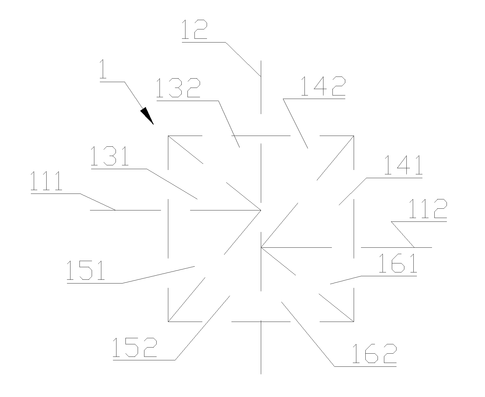
One embodiment of the present invention discloses a method for pixel arrangement and a display using the same. The display areas are divided into a plurality of rectangular regions which have the same area according to a plurality of vertical grids which own the same distance between the adjacent. According to pre-positioning horizontal axis lines and pre-positioning vertical axis lines, each of the rectangular regions is divided into four parts including an upper left part, an upper right part, a lower left part and a lower right part. Each of the four parts are divided into two sub-pixel areas by a line which is inside the part. The line connects the angle point of the region which the part belongs to and the cross point of the horizontal axis line and the vertical axis line of the region which the part belongs to.

Description

CROSS-REFERENCE TO RELATED APPLICATIONS[0001]The present application claims priority to and the benefit of Chinese Patent Application No. CN 201310292428.3, filed on Jul. 11, 2013, the entire content of which is incorporated herein by reference.BACKGROUND OF THE INVENTION[0002]1. Field of the Invention[0003]The present disclosure is related to the technology of pixel arrangement, more specifically, to a method for pixel arrangement and a display using the same.[0004]2. Description of the Related Art[0005]OLED, i.e., Organic Light-Emitting Diode, is also named as Organic Electroluminescence Display. OLED owns a character of self-luminous, which is achieved by the light-emitting of thin organic material coatings on the glass substrate where the current passing. The visual angle of OLED display screen is large and the electric energy could be economized greatly. Hence, OLED owns some advantages that other display screens do not have.[0006]However, due to the limitation of the manufactu...

Claims


Application Information

Patent Timeline
Patent Type & Authority Applications(United States)
IPC IPC(8): H01L27/32H01L51/56
CPCH01L51/56H01L27/3218H01L27/3262H10K59/353H10K59/352
Inventor HUANG, TIANWANGWU, CHIENLIN
Owner EVERDISPLAY OPTRONICS (SHANGHAI) CO LTD
Learn More