

Fingerprint sensing system and method
a fingerprint and sensing technology, applied in the field of fingerprint sensing systems, can solve the problems of requiring a relatively large capacitance, unable to fully compensate for the variation in reference potential using the driving signal, and the fingerprint image is difficult to analyze, so as to improve the fingerprint sensing and improve the sensing
- Summary
- Abstract
- Description
- Claims
- Application Information
AI Technical Summary
Benefits of technology
Problems solved by technology
Method used
Image

Examples
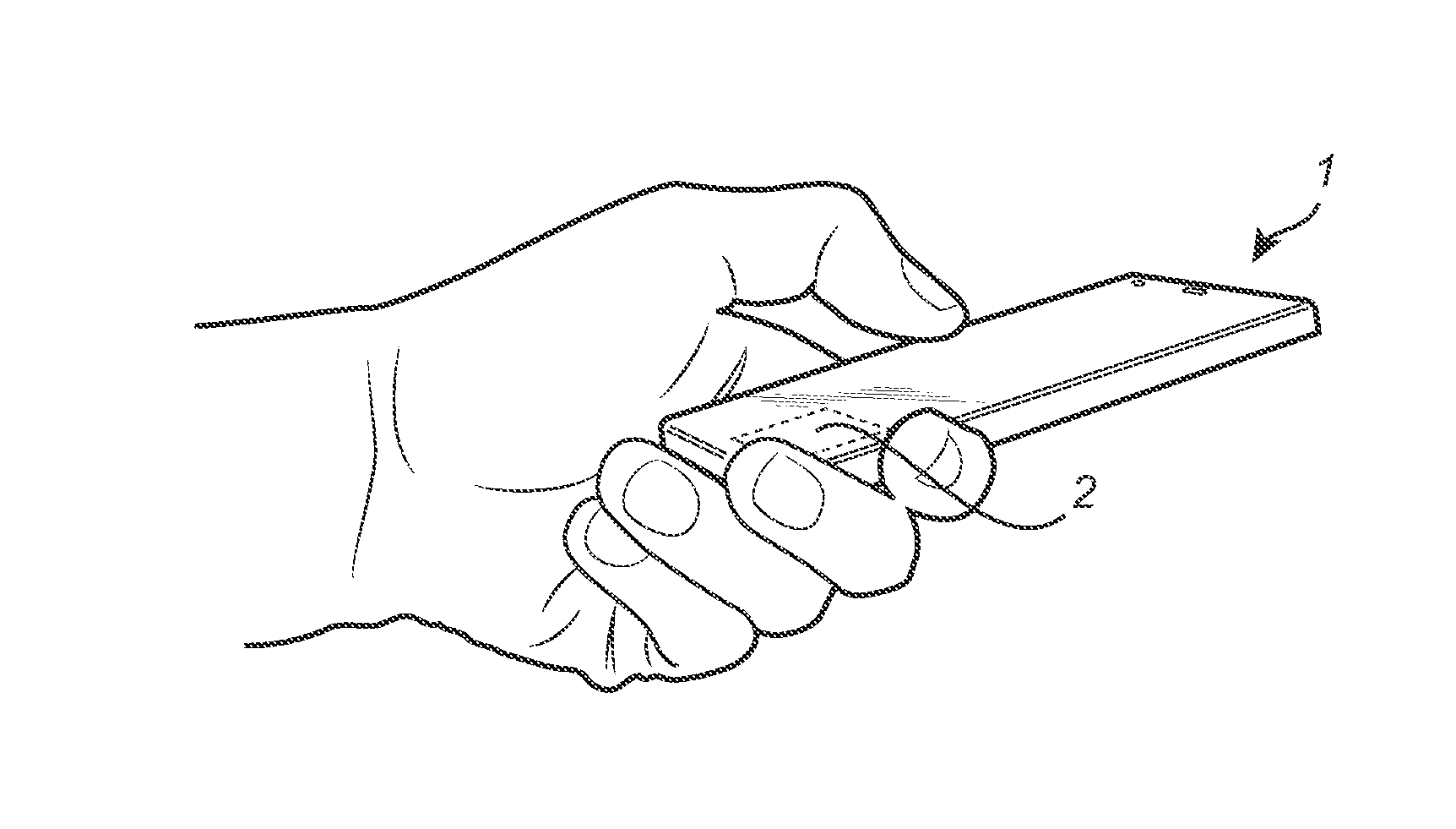
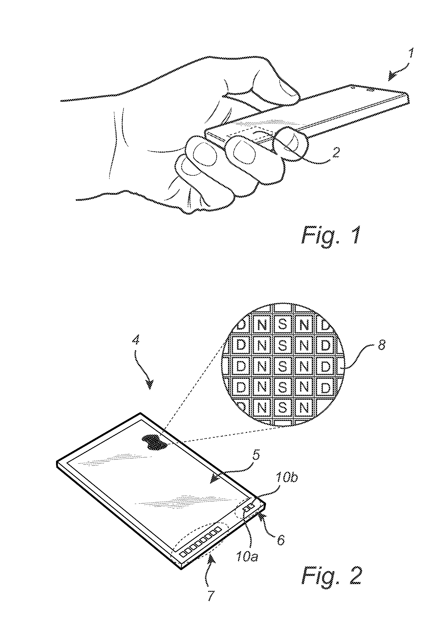
first embodiment
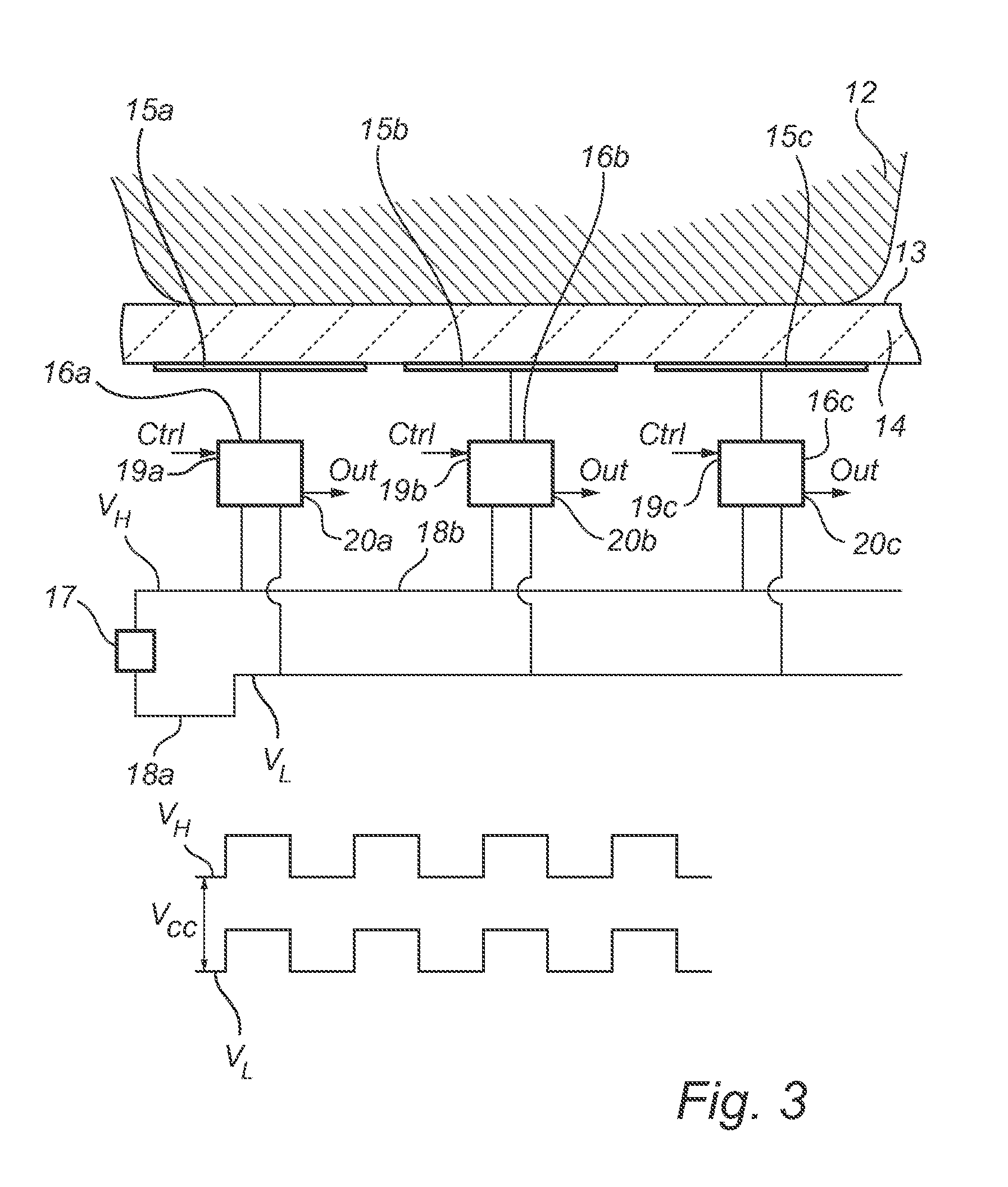
[0104]In this first embodiment, the fingerprint sensing system 2 does not comprise any external structure for electrically contacting the finger 12. For the fingerprint sensing system 2 in FIG. 5, it may therefore be beneficial to reduce unwanted capacitive drive, for example as described above with reference to FIG. 4.
[0105]As is schematically indicated using a box with dashed line boundaries, the fingerprint sensing system 2 may optionally additionally include isolation circuitry 29 for providing galvanic isolation or level shifting between the sensor array 5 and the microprocessor 25. Through the use of isolation circuitry 29, the microprocessor 25 is allowed to work independently of the varying, in relation to DGND, reference potential VL of the sensor array 5.
[0106]As was mentioned in the Summary section, the isolation circuitry 29 can be implemented in many different ways known to the skilled person. For instance, the isolation circuitry 29 may be implemented using components ...
second embodiment
[0118]FIG. 8b schematically shows the sensor voltage source 27 comprising an input 39, a diode 40 and a capacitor 41. The diode 40 is connected between the input 39 of the sensor voltage source 27 and the high potential input of the fingerprint sensor 4, and the capacitor 41 is connected between the low potential VL and the high potential VH of the supply voltage for the fingerprint sensor 4. The input 39 is for connection of the supply voltage Vcc of the device comprising the fingerprint sensing system 2 as was described above with reference to FIGS. 7a-c.
[0119]The isolation circuit in FIG. 8b does not provide full galvanic isolation between the supply voltage Vcc and the fingerprint sensor 4, but enables the provision of time-varying low potential VL and high potential VH to the fingerprint sensor 4 even though the supply voltage (or rather supply potential) Vcc remains constant.
[0120]It should be noted that the voltage source 37 in FIG. 8a as well as the supply voltage VCC provi...
PUM
 Abstract
Description
Claims
Application Information