Array substrate, method of disconnection inspecting gate lead wire and source lead wire in the array substrate, method of inspecting the array substrate, and liquid crystal display device

a technology of array substrate and array substrate, which is applied in the direction of static indicating devices, semiconductor/solid-state device details, instruments, etc., can solve the problems of increasing the number of probes constructing a probe unit, failure of semiconductor switching elements, and narrowing of probe intervals

Active Publication Date: 2015-01-15
TRIVALE TECH
View PDF2 Cites 10 Cited by
  • Summary
  • Abstract
  • Description
  • Claims
  • Application Information

AI Technical Summary

Benefits of technology

[0013]An object of the present invention is to provide an array substrate which can be inspected before the array substrate is overlapped with an opposed substrate without being influenced by increase in the density of semiconductor chips, and in which inspection for disconnection in lead wires from mounting terminals of semiconductor chips to the inside of a display region can be performed.
[0015]In the array substrate according to the present invention, since the source-side array inspection terminals and the gate-side array inspection terminals are provided in regions different from those of the gate-driver mounting terminals and the source-driver mounting terminals, a probe unit can be manufactured without restriction of the probe intervals, and even in the case of using a high-density semiconductor chip, a wiring inspection can be performed. Further, by providing the gate lead wire disconnection inspection circuits and the source lead wire disconnection inspection circuits, disconnection in the lead wires (the gate lead wires and the source lead wires) from the display region to the mounting terminals can be detected. Therefore, a faulty array substrate is not proceeded to the later manufacturing process, so that unnecessary process cost and use of members can be reduced, and the manufacturing cost can be decreased.

Problems solved by technology

Concretely, by writing charges in pixels constructing a display region and reading the charges, an inspection for disconnection in a gate signal line and a source signal line in a semiconductor switching element, a defect of a pixel, and a failure of a semiconductor switching element is performed.
As the resolution of display panels is becoming higher and the density of semiconductor chips is becoming higher, there is the tendency that the number of probes constructing a probe unit increases, and the probe interval becomes narrower, and it is becoming difficult to fabricate the probe unit.
However, as the size of semiconductor chips is becoming smaller and the frame of the display panels is becoming narrower, the size of the semiconductor chip mounting region has to be decreased.
However, a problem occurs such that an inspection for disconnection in lead wires from mounting terminals of semiconductor chips to a display plane cannot be performed.
There is, consequently, a problem such that in the case where it is found out that something is wrong with the array substrate at this manufacturing stage, the opposed substrate, the liquid crystal, and the cost of the manufacture up to the stage are wasted.

Method used


Image

  • Array substrate, method of disconnection inspecting gate lead wire and source lead wire in the array substrate, method of inspecting the array substrate, and liquid crystal display device
  • Array substrate, method of disconnection inspecting gate lead wire and source lead wire in the array substrate, method of inspecting the array substrate, and liquid crystal display device
  • Array substrate, method of disconnection inspecting gate lead wire and source lead wire in the array substrate, method of inspecting the array substrate, and liquid crystal display device

Examples


first preferred embodiment

Configuration

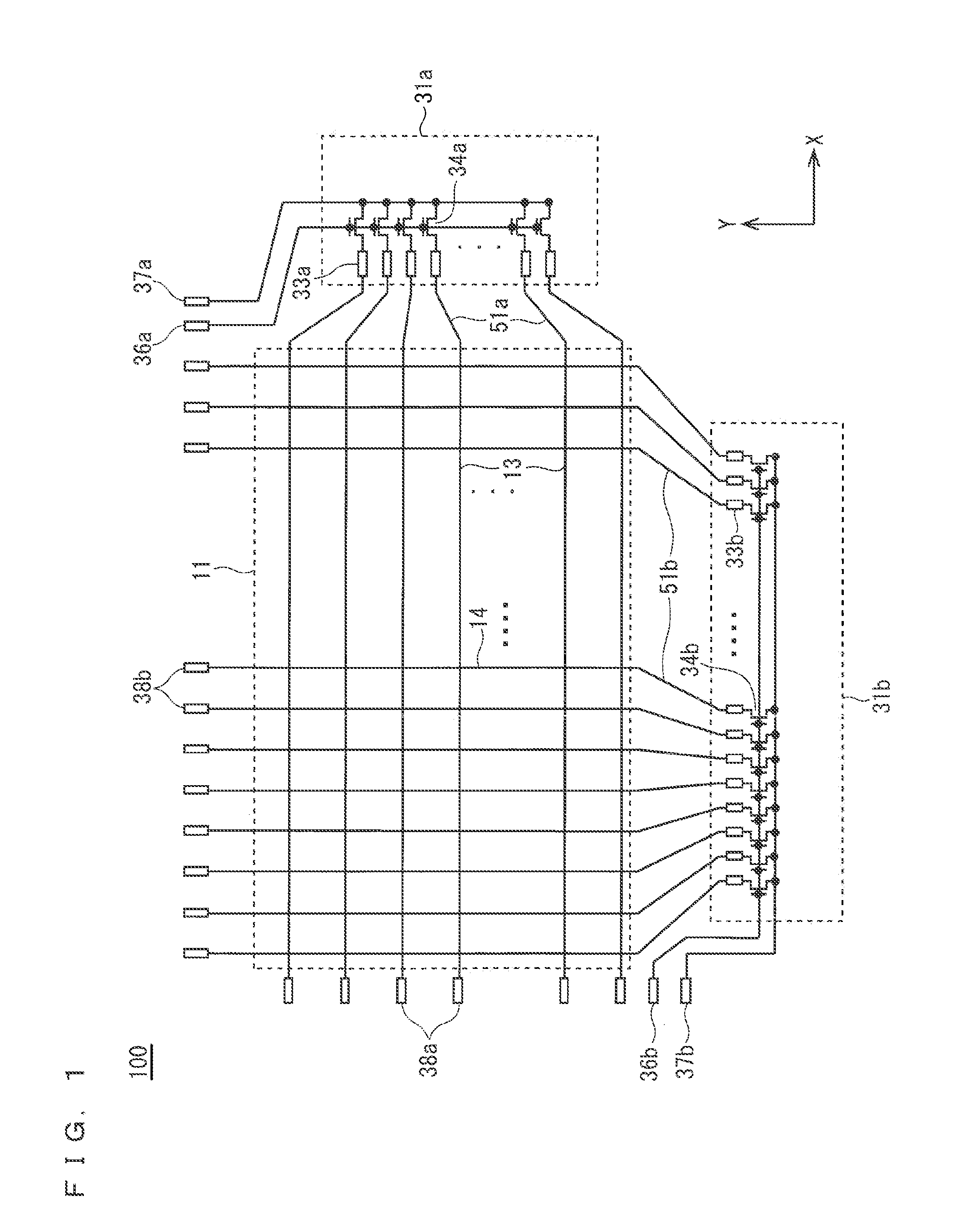
[0024]FIG. 1 is a plan view of an array substrate 100 for a liquid crystal panel in the first preferred embodiment. As illustrated in FIG. 1, the array substrate 100 includes a display region 11 displayed by broken lines, semiconductor chip mounting regions (that is, a gate-driver mounting region 31a and a source-driver mounting region 31b), gate-side array inspection terminals 38a, and source-side array inspection terminals 38b.

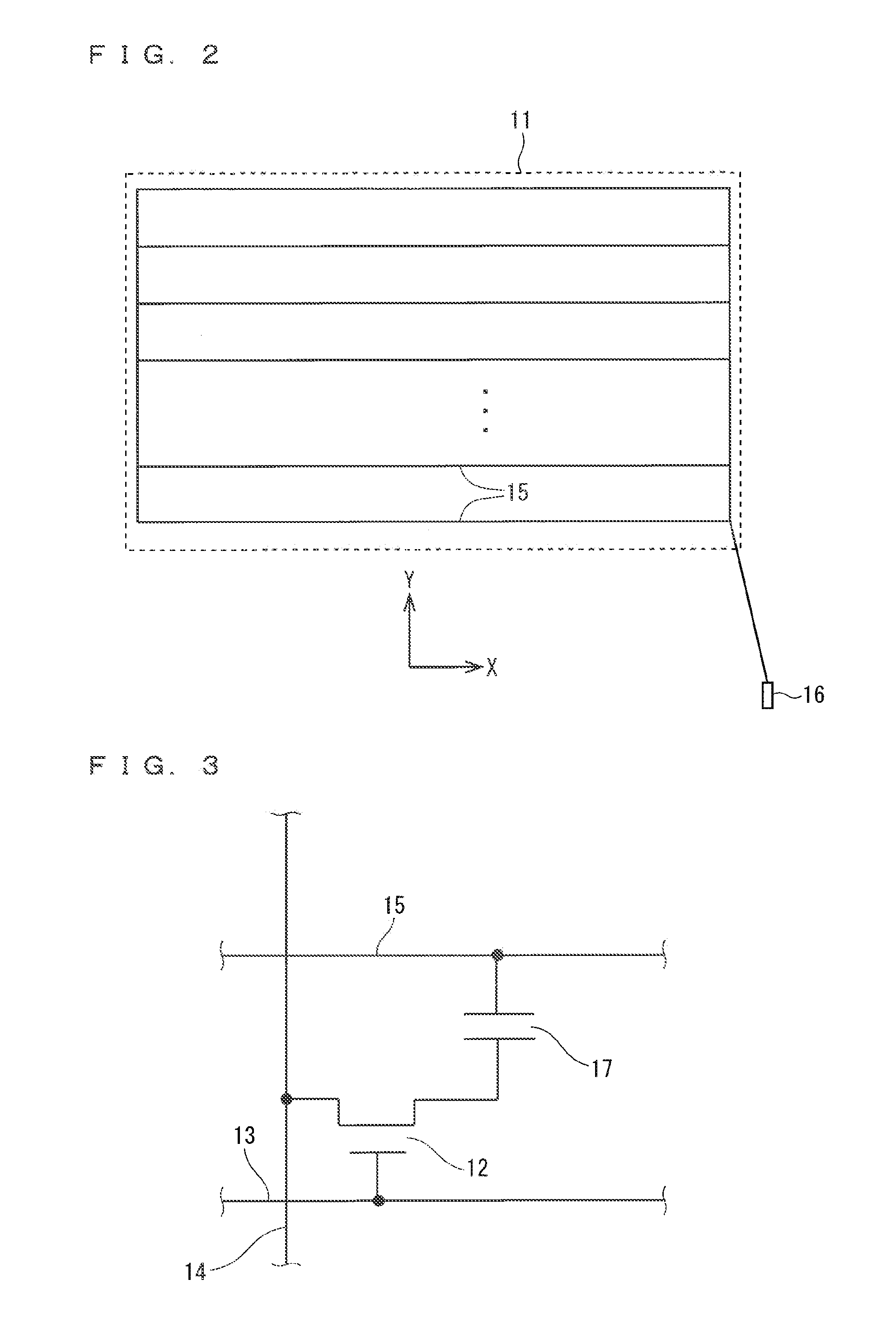
[0025]The display region 11 is provided with a plurality of gate signal lines 13 and a plurality of source signal lines 14. The plurality of gate signal lines 13 extend in the X direction and are arranged in parallel in the Y direction. The plurality of source signal lines 14 extend in the Y direction and are arranged in parallel in the X direction. As illustrated in FIG. 2, a plurality of common wires 15 are provided at intervals equivalent to those of the gate signal lines 13, and the common wires 15 are electrically connected. For simplicity...

second preferred embodiment

Configuration

[0053]FIG. 4 is a plan view of an array substrate 200 according to a second preferred embodiment. In the first preferred embodiment (FIG. 1), the gate-side TFTs 34a are used as the gate lead wire disconnection inspection circuits, and the source-side TFTs 34b are used as the source lead wire disconnection inspection circuits. On the other hand, in the second preferred embodiment, resistive elements 41a and 41b are used as a gate lead wire disconnection inspection circuit and a source lead wire disconnection inspection circuit. Although the gate-side switch terminal 36a and the source-side switch terminal 36b are provided to control the gate-side TFTs 34a and the source-side TFTs 34b in the first preferred embodiment, since the resistive elements are used in the second preferred embodiment, they are unnecessary in the second embodiment. For simplicity of the drawing, the common wires 15 are not illustrated in FIG. 4. The configuration of the common wire 15 is similar to ...

third preferred embodiment

Configuration

[0070]FIG. 6 is a plan view of an array substrate 300 in a third preferred embodiment. In the second preferred embodiment, the resistive elements 41a and 41b are used as the gate lead wire disconnection inspection circuit and the source lead wire disconnection inspection circuit. On the other hand, in the third preferred embodiment, capacitive elements 42a and 42b are used as the gate lead wire disconnection inspection circuit and the source lead wire disconnection inspection circuit. In FIG. 6, for simplicity of the drawing, the common wires 15 are not illustrated. The configuration of the common wires 15 is similar to that of FIG. 2. Since the other configuration is similar to that of the second preferred embodiment, the description will not be repeated.

[0071]In the case of constructing, for example, a liquid crystal display device by using the array substrate 300 illustrated in FIG. 6, in a manner similar to the first preferred embodiment, liquid crystal is sealed in...


PUM

PropertyMeasurementUnit
voltagesaaaaaaaaaa
voltageaaaaaaaaaa
densityaaaaaaaaaa

Abstract

An array substrate has a plurality of gate signal lines, a plurality of source signal lines orthogonal to the plurality of gate signal lines, a plurality of gate-driver mounting terminals, a plurality of source-driver mounting terminals, a plurality of gate-side array inspection terminals connected to the gate signal lines, a plurality of source-side array inspection terminals connected to the source signal lines, a plurality of gate lead wire disconnection inspection circuits connected between the plurality of gate-driver mounting terminals and a common terminal for a gate lead wire disconnection inspection, and a plurality of source lead wire disconnection inspection circuits connected between the plurality of source-driver mounting terminals and a common terminal for a source lead wire disconnection inspection.

Description

BACKGROUND OF THE INVENTION[0001]1. Field of the Invention[0002]The present invention relates to an array substrate, method of disconnection inspecting a gate lead wire and a source lead wire in the array substrate, a method of inspecting the array substrate, and a liquid crystal display device.[0003]2. Description of the Background Art[0004]In process of manufacturing a liquid crystal display panel, an inspection of disconnection in an array substrate in which a circuit for display is formed on glass, a defect of a pixel, or the like is performed. Concretely, by writing charges in pixels constructing a display region and reading the charges, an inspection for disconnection in a gate signal line and a source signal line in a semiconductor switching element, a defect of a pixel, and a failure of a semiconductor switching element is performed.[0005]The inspection is generally sequentially performed by bringing probes into contact with inspection terminals provided for gate signal line...

Claims


Application Information

Patent Timeline
Patent Type & Authority Applications(United States)
IPC IPC(8): G01R31/28H01L27/12G02F1/1362
CPCG02F1/136286G02F2001/136254G01R31/2884H01L27/124G02F1/1309G02F1/1345G09G3/006G09G3/3648G02F1/136254
Inventor MASUTANI, YUICHIMURAKAMI, KATSUAKI
Owner TRIVALE TECH
Why Eureka
Try Eureka