Chip resistor and mounting structure thereof

a technology of mounting structure and resistor, which is applied in the direction of resistors, resistor details, electrical devices, etc., can solve the problem that the heat generated in the resistor cannot be efficiently dissipated to the outside, and achieve the effect of improving heat dissipation efficiency

Active Publication Date: 2015-01-22
ROHM CO LTD
View PDF8 Cites 3 Cited by
  • Summary
  • Abstract
  • Description
  • Claims
  • Application Information

AI Technical Summary

Benefits of technology

The objective of this patent is to create a chip resistor with better ability to spread out or absorb heat.

Problems solved by technology

This patent discusses different types of resistors with plates and electrodes. However, these conventional methods have limitations when making a resistor with high resistance because it requires increasing the space between the electrodes, resulting in smaller electrodes that can't effectively dissipate heat. Therefore, there is a technical problem related to efficient heat dissipation while maintaining high resistance levels.

Method used


Image

  • Chip resistor and mounting structure thereof
  • Chip resistor and mounting structure thereof
  • Chip resistor and mounting structure thereof

Examples


first embodiment

[0065]the present invention is described below with reference to FIGS. 1-18.

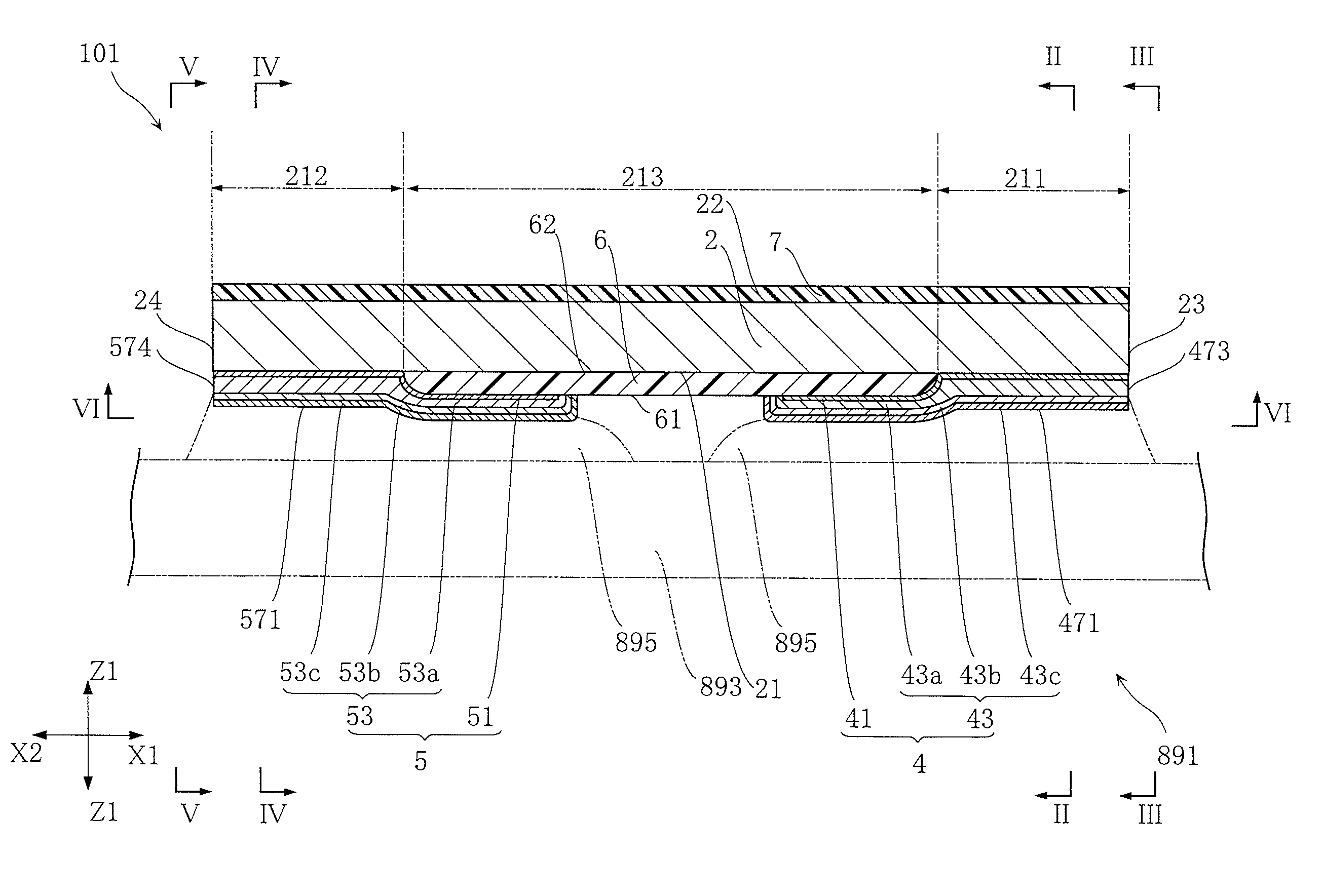
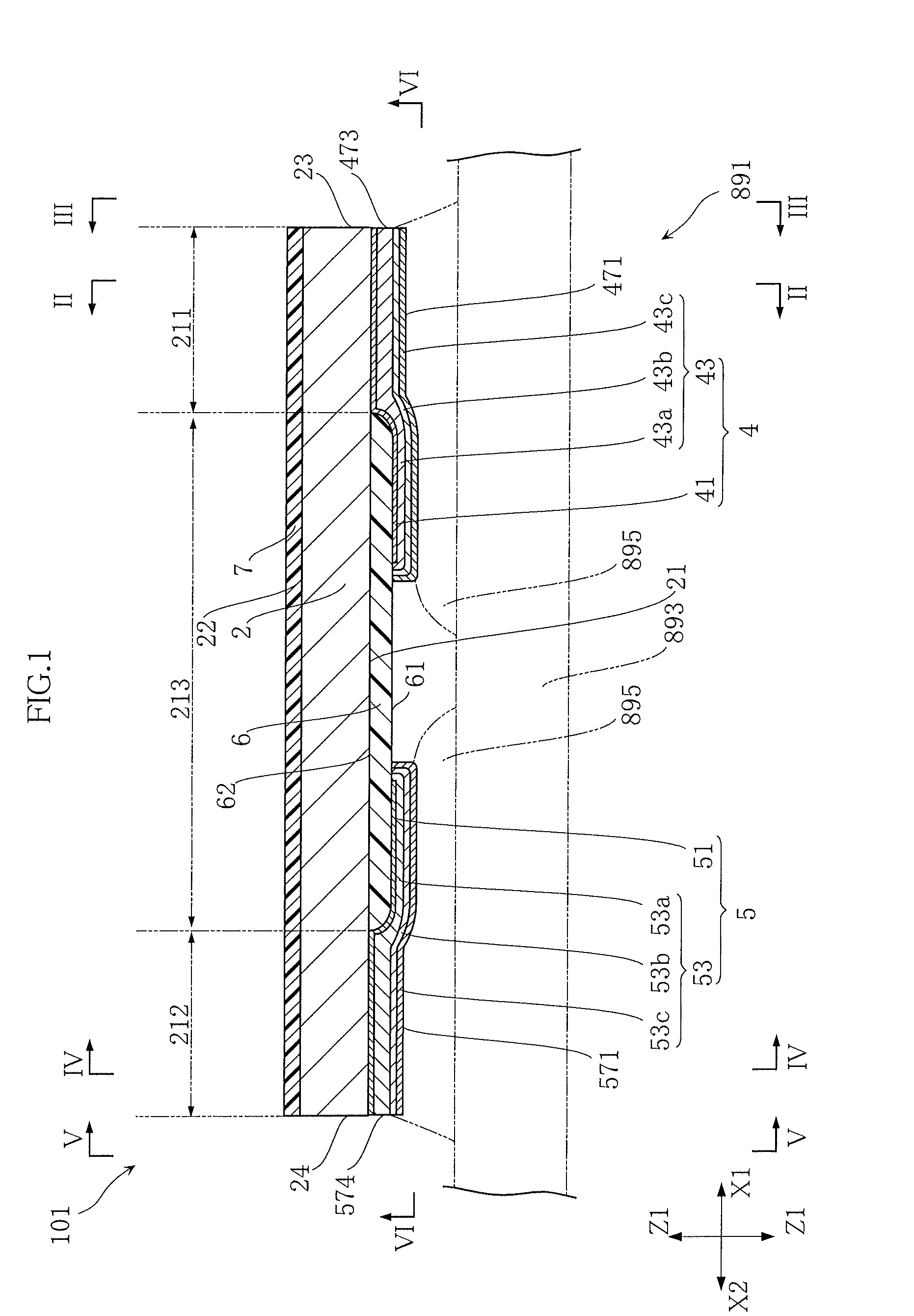
[0066]FIG. 1 is a sectional view illustrating amounting structure of a chip resistor according to a first embodiment of the present invention.

[0067]The chip resistor mounting structure 891 illustrated in the figure includes a chip resistor 101, a mount board 893 and an electroconductive bonding portion 895.

[0068]For instance, the mount board 893 is a printed circuit board including an insulating substrate and a pattern electrode (not shown) formed on the insulating substrate. For instance, the insulating substrate is a glass epoxy resin substrate. The chip resistor 101 is mounted on the mount board 893. The electroconductive bonding portion 895 is provided between the chip resistor 101 and the mount board 893. The electroconductive bonding portion 895 bonds the chip resistor 101 and the mount board 893 to each other. For instance, the electroconductive bonding portion 895 comprises solder.

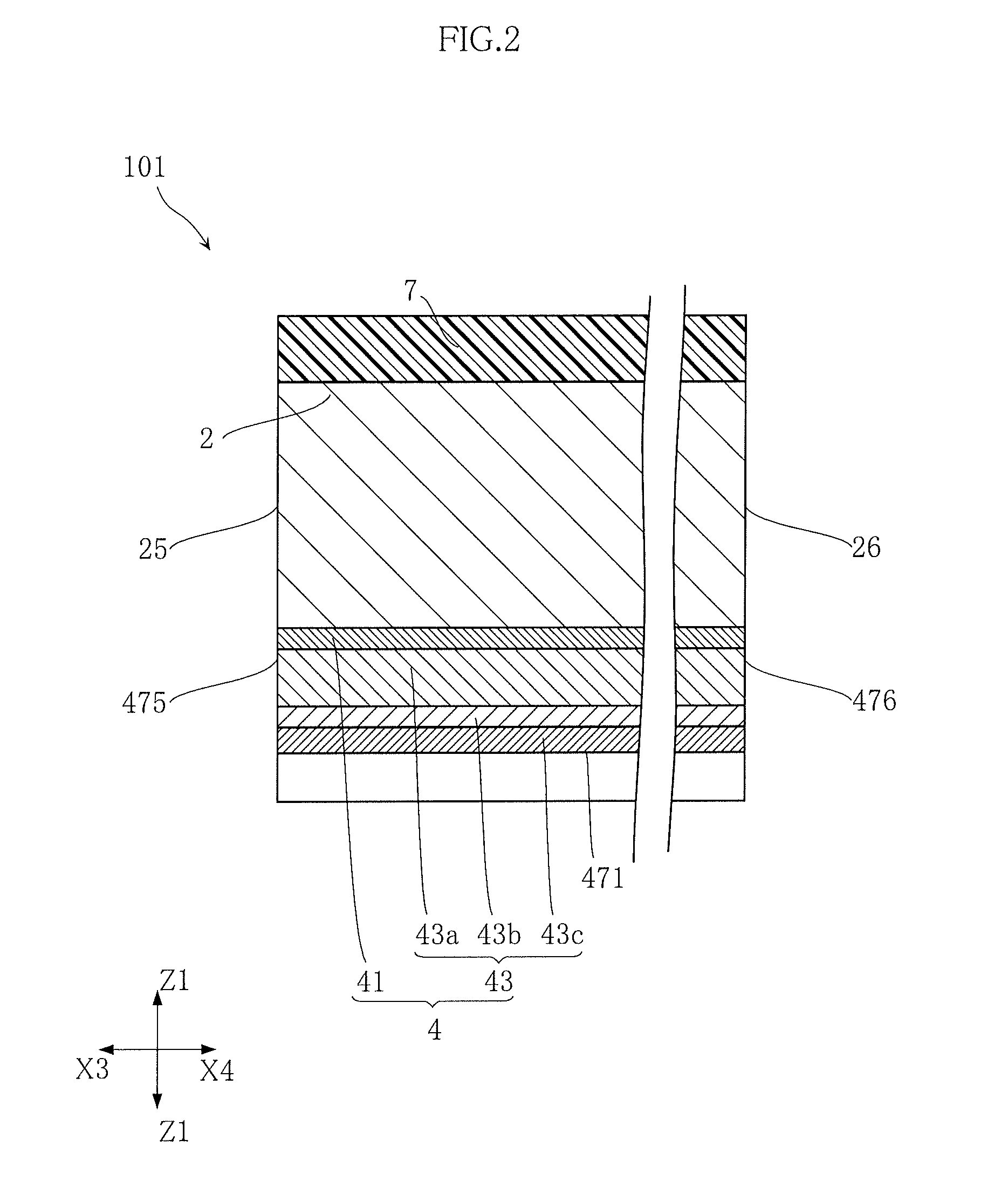
[0069]FIG. 2 is a s...

second embodiment

[0123]the present invention is described below with reference to FIGS. 19-25.

[0124]In the description given below, the elements that are identical or similar to those of the foregoing embodiments are designated by the same reference signs as those used for the foregoing embodiments and the explanation is omitted appropriately.

[0125]FIG. 19 is a sectional view illustrating a mounting structure of a chip resistor according to a second embodiment of the present invention.

[0126]The chip resistor mounting structure 892 illustrated in the figure includes a chip resistor 102, a mount board 893 and an electroconductive bonding portion 895.

[0127]Since the structures of the mount board 893 and the electroconductive bonding portion 895 are the same as those of the first embodiment, explanation of these portions is omitted.

[0128]FIG. 20 is a sectional view of the chip resistor taken along lines XX-XX in FIG. 19. FIG. 21 illustrates the chip resistor as viewed in the direction of arrows XXI-XXI ...


PUM


Abstract

A chip resistor includes a resistor board, a first electrode, a second electrode and an insulating layer. The second electrode is offset from the first electrode in a lateral direction perpendicular to the thickness direction of the resistor board. The obverse surface of the resistor board includes a first region in contact with the first electrode, a second region in contact with the second electrode and an intermediate region in contact with the insulating layer. The intermediate region is disposed between the first region and the second region in the lateral direction. The first electrode includes a first underlying layer and a first plating layer. The first underlying layer is disposed between the first plating layer and the insulating layer in the thickness direction of the resistor board.

Description


Claims


Application Information

Patent Timeline
Owner ROHM CO LTD
Why Eureka
Try Eureka