Mos transistors and fabrication method thereof

a technology of transistors and fabrication methods, applied in the direction of basic electric elements, electrical equipment, semiconductor devices, etc., can solve the problem that the hkmg structure of the transistor b>20/b> may have a relatively high leakage curren

Active Publication Date: 2015-02-05
SEMICON MFG INT (SHANGHAI) CORP
View PDF6 Cites 23 Cited by
  • Summary
  • Abstract
  • Description
  • Claims
  • Application Information

AI Technical Summary

Benefits of technology

This patent describes how to make an improved type of electronic component called a MOS transistor. A new technique was used that involved creating a special material around the part where other materials would be added later during production. By doing this, researchers were able to better control the growth of these materials which resulted in more reliable and efficient components.

Problems solved by technology

The patent text discusses a problem with the current process of forming MOS transistors with a high-K metal gate (HKMG structure). The current process results in a relatively high leakage current, which needs to be addressed. The disclosed device structures and methods aim to solve this problem.

Method used


Image

  • Mos transistors and fabrication method thereof
  • Mos transistors and fabrication method thereof
  • Mos transistors and fabrication method thereof

Examples


Embodiment Construction

[0013]Reference will now be made in detail to exemplary embodiments of the invention, which are illustrated in the accompanying drawings. Wherever possible, the same reference numbers will be used throughout the drawings to refer to the same or like parts.

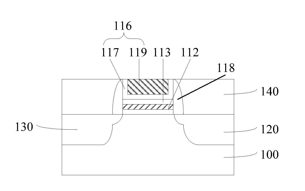
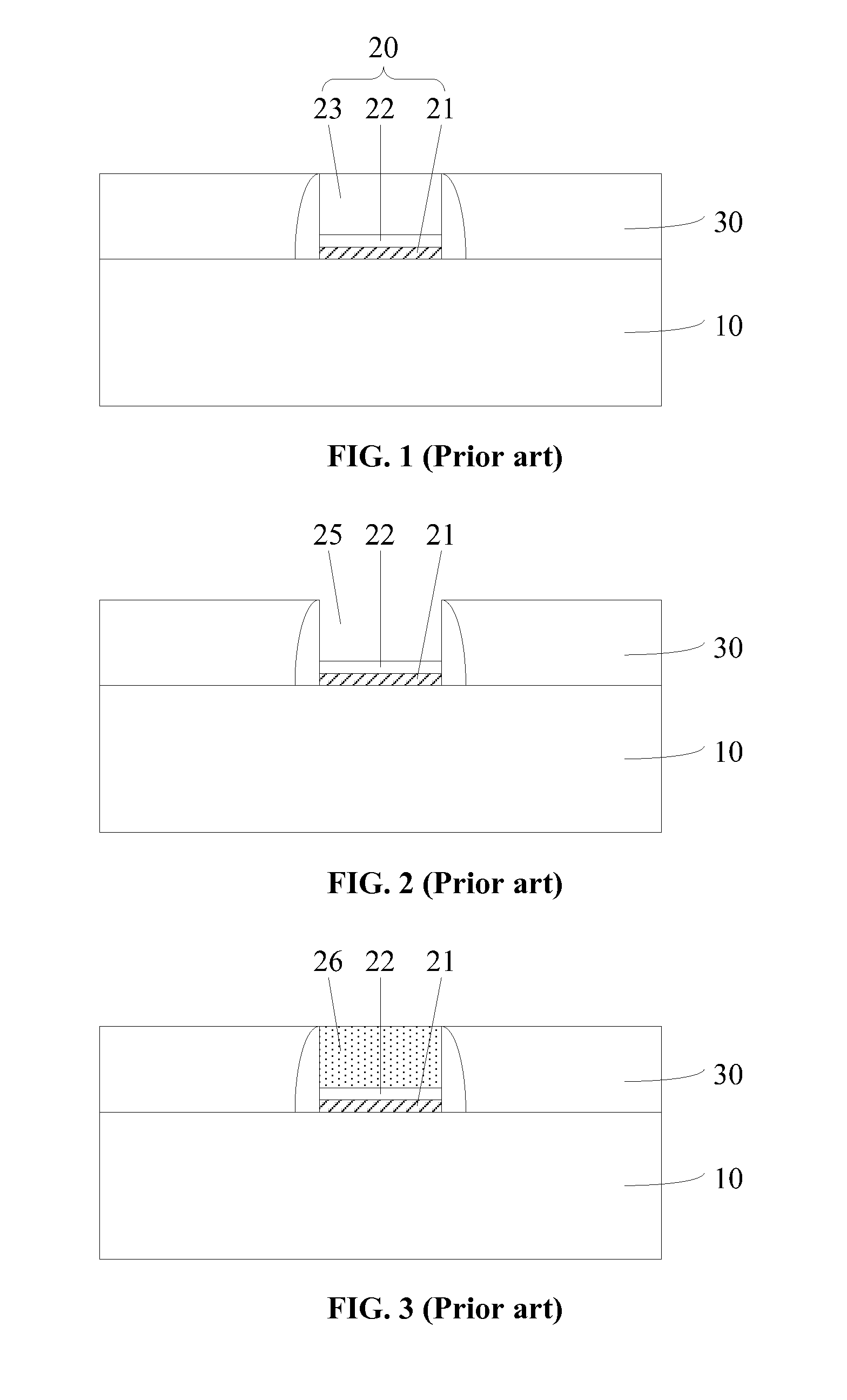
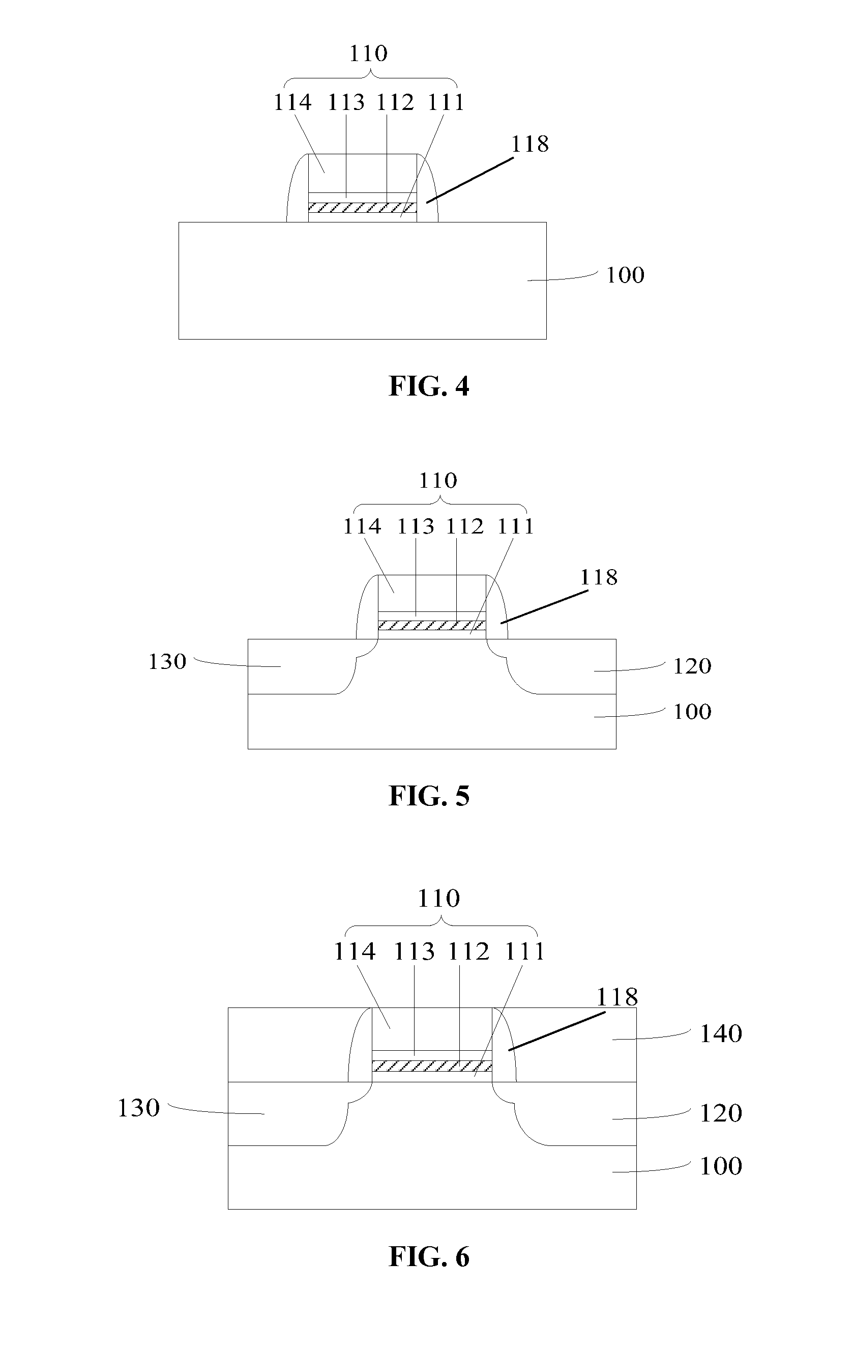
[0014]A high-K gate dielectric layer and a high-K gate dielectric protection layer may be included in a poly silicon dummy gate structure, when the poly silicon gate of the poly silicon dummy gate structure is removed by an etching process, the high-K gate dielectric protection layer may be over etched by the etching process. Especially when high-K gate dielectric protection layer contains nitrogen, nitrogen bonds may be damaged by the over etching; and defects may be formed. A MOS transistor having such a high-K metal gate structure may have a relatively large leakage current. The present invention overcomes this problem and other related problems by repairing the high-K gate dielectric protection layer using a nitrogen treatment ...


PUM


Abstract

A method is provided for fabricating an MOS transistor. The method includes providing a semiconductor substrate; and forming a ploy silicon dummy gate structure having a high-K gate dielectric layer, a high-K gate dielectric protection layer containing nitrogen and a poly silicon dummy gate on the semiconductor substrate. The method also includes forming a source region and a drain region in the semiconductor substrate at both sides of the poly silicon dummy gate structure. Further, the method includes removing the poly silicon dummy gate to form a trench exposing the high-K gate dielectric protection layer containing nitrogen and performing a nitrogen treatment process to repair defects in the high-K gate dielectric protection layer containing nitrogen caused by removing the poly silicon dummy gate. Further, the method also includes forming a metal gate structure in the trench.

Description


Claims


Application Information

Patent Timeline
Owner SEMICON MFG INT (SHANGHAI) CORP
Why Eureka
Try Eureka