Solid-state imaging element and manufacturing method for solid-state imaging element

a manufacturing method and imaging element technology, applied in the direction of solid-state devices, transistors, radio-controlled devices, etc., can solve the problems of residual image in image data, deterioration in read efficiency of electric charges from charge storage regions into read regions, etc., to reduce potential barrier in channel regions, suppress residual image occurren

Active Publication Date: 2015-03-05
SHARP KK
View PDF3 Cites 2 Cited by
  • Summary
  • Abstract
  • Description
  • Claims
  • Application Information

AI Technical Summary

Benefits of technology

[0030]According to the solid-state imaging element with the above characteristics, it becomes possible to reduce the potential barrier in the channel region while providing the shield region for suppressing a dark current and a white spot. Hence it becomes possible to suppress occurrence of a dark current and a white spot and even suppress occurrence of a residual image. Further, according to the manufacturing method for the solid-state imaging element with the above characteristics, it becomes possible to suppress relative displacement, so as to accurately manufacture the solid-state imaging element which can suppress occurrence of a dark current and a white spot and can even suppress occurrence of a residual image.

Problems solved by technology

Such a solid-state imaging element has a problem of a dark current and a white spot which occur due to electric charges generated not by incidence with light (a phenomenon of a white signal being generated by a large amount of dark current).
At this time, a potential in the shield region becomes significantly large as compared to a potential in the charge storage region, thus leading to deterioration in read efficiency of the electric charges from the charge storage region into the read region.
When a large amount of electric charges cannot be read and left in the charge storage region, those electric charges are mixed with electric charges that are stored in the next photoelectric conversion to cause occurrence of a residual image in image data, which is problematic.

Method used


Image

  • Solid-state imaging element and manufacturing method for solid-state imaging element
  • Solid-state imaging element and manufacturing method for solid-state imaging element
  • Solid-state imaging element and manufacturing method for solid-state imaging element

Examples


Embodiment Construction

Structural Example of Solid-State Imaging Element

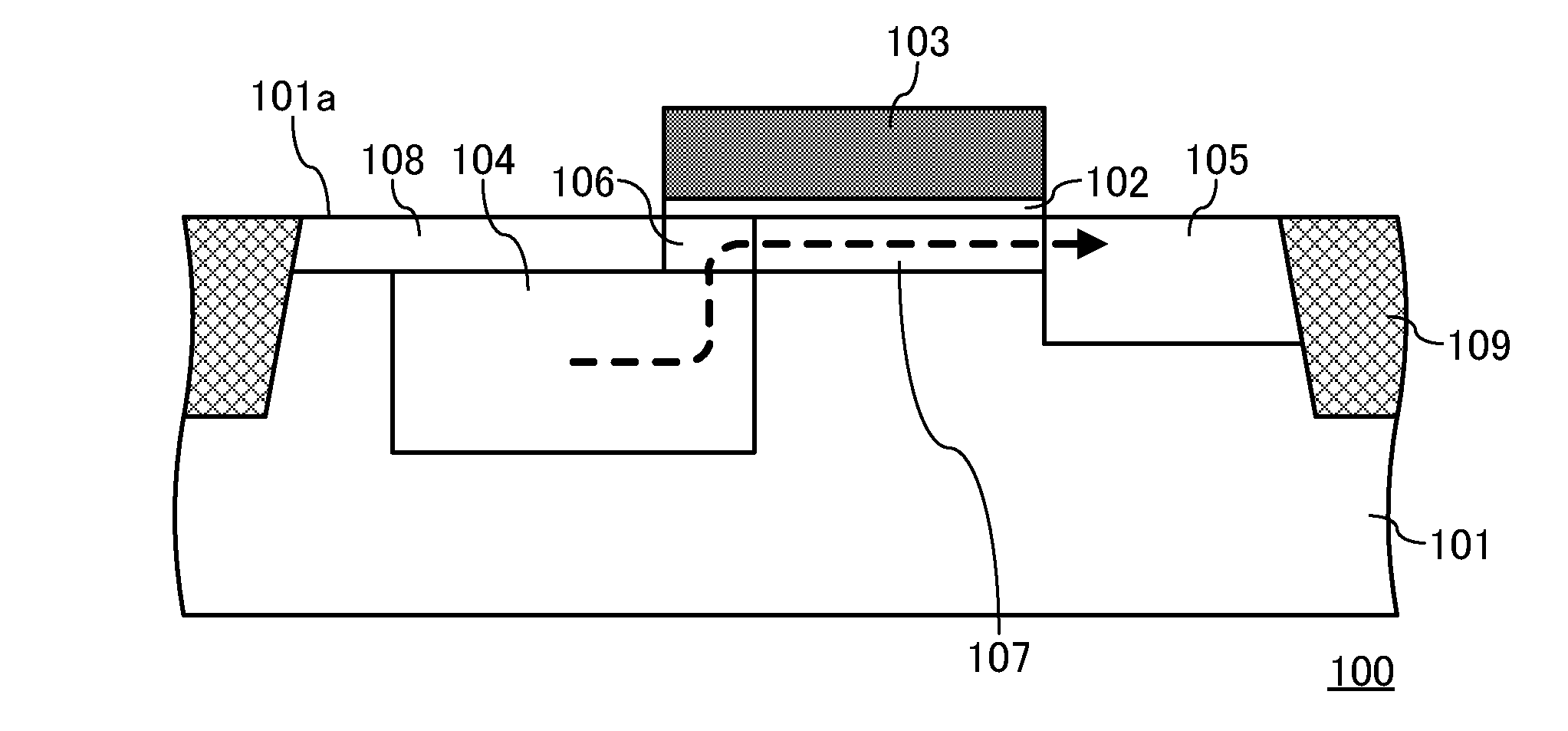
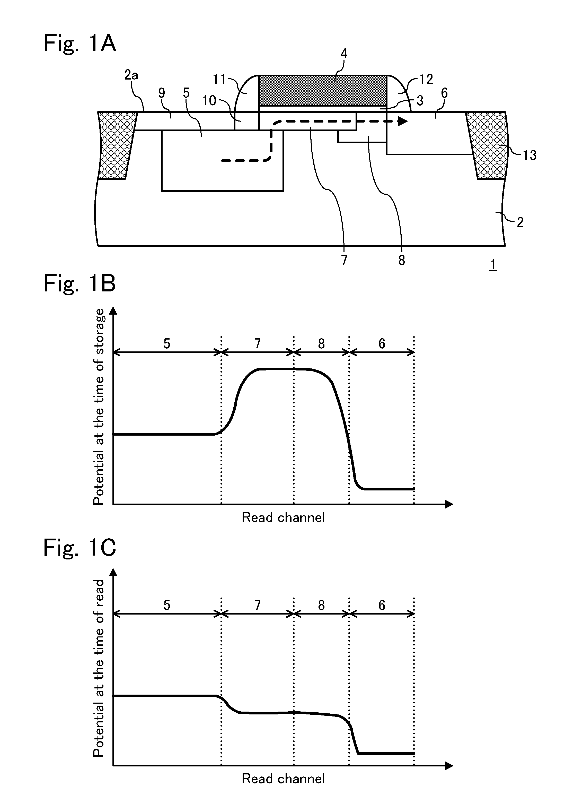
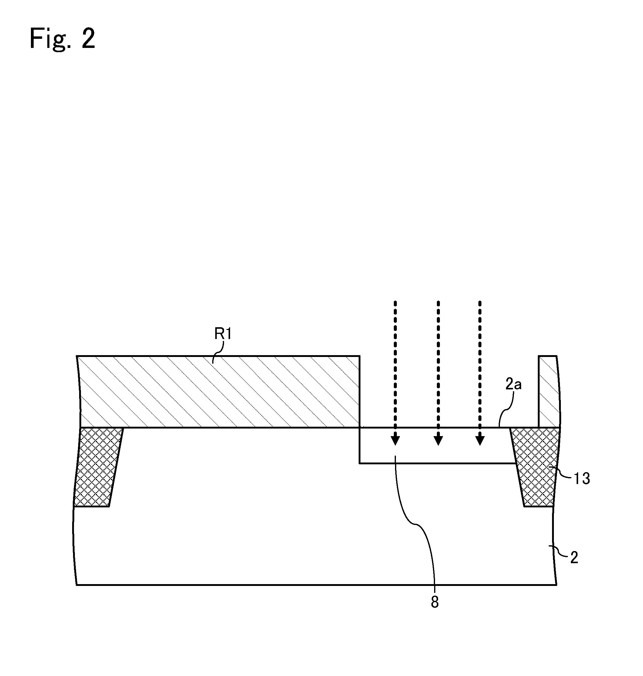
[0041]A structural example of a solid-state imaging element according to an embodiment of the present invention will be described with reference to the drawings. However, for embodying the description, a case will be shown hereinafter where a solid-state imaging element as a CMOS image sensor is provided with an n-type charge storage region in a p-type substrate, and the charge storage region stores electrons. It is to be noted that the “p-type substrate” means a substrate where a portion to be formed with an element structure is the p type, and it is not restricted to a substrate being entirely the p type, but it naturally includes a substrate with a well being the p type (e.g., a substrate which is formed with a p-type well by injecting the p-type impurities into a substrate being entirely the n type). However, it is assumed that in each drawing to be referenced in the following description, the substrate is illustrated as if being ...


PUM


Abstract

Provided are a solid-state imaging element, which suppresses occurrence of a dark current and a white spot and even suppresses occurrence of a residual image, and a manufacturing method for the solid-state imaging element. A solid-state imaging element (1) is provided with: a gate electrode (4) above a substrate (2); a charge storage region (5) formed at a position inside the substrate (2) and apart from a top surface (2a) of the substrate (2); a read region (6) formed at a position inside the substrate (2) and on the opposite side to the charge storage region (5) with the gate electrode (4) interposed therebetween; a channel region (7, 8) formed inside the substrate (2) and immediately below the gate electrode (4); and a shield region (9) and an intermediate region (10) formed inside the substrate (2) and between the top surface (2a) of the substrate (2) and the charge storage region (5). The intermediate region (10) is formed at a position inside the substrate (2) and between the channel region (7, 8) and the shield region (9), and is in contact with each of the channel region (7, 8) and the shield region (9), and a concentration of first conductive type impurities in the intermediate region (10) is lower than a concentration of the first conductive type impurities in the shield region (9).

Description

TECHNICAL FIELD[0001]The present invention relates to a solid-state imaging element represented by a CMOS (Complementary Metal Oxide Semiconductor) image sensor, a CCD (Charge Coupled Device) image sensor and the like, and a manufacturing method for the solid-state imaging element.BACKGROUND ART[0002]In recent years, solid-state imaging elements such as a CCD image sensor and a CMOS image sensor are mounted in imaging devices such as a digital video camera and a digital still camera, and a variety of electronic equipment provided with an imaging function, such as a scanner, a facsimile and a cell phone with a camera. For example, the solid-state imaging element stores, in a charge storage region forming part of the photodiode, electric charges generated by photoelectric conversion of a photodiode formed in a substrate, and also generates a signal constituting image data based on the electric charges read from the charge storage region into a read region at predetermined timing.[0003...

Claims


Application Information

Patent Timeline
Patent Type & Authority Applications(United States)
IPC IPC(8): H01L27/146
CPCH01L27/14616H01L27/14643H01L27/14689H01L27/1461
Inventor OHTSUBO, KAZUO
Owner SHARP KK
Why Eureka
Try Eureka