
Shallow junction photovoltaic devices

Inactive Publication Date: 2015-03-12
GLOBALFOUNDRIES INC
View PDF3 Cites 19 Cited by
  • Summary
  • Abstract
  • Description
  • Claims
  • Application Information

AI Technical Summary

Benefits of technology

The patent text describes a method and device for making a photovoltaic device. The method involves creating contacts on a crystalline substrate with specific doping concentrations, dislocation densities, and hydrogen content to maximize the efficiency of the device. A passivation layer is then added to reduce recombination in the epitaxially grown layers. The device itself consists of the contacts and a passivation layer, which help to improve the performance of the photovoltaic device.

Problems solved by technology

In addition, doping levels below 1019 cm−3 do not completely shield the carriers from the substrate surface, therefore limiting the Voc due to recombination at localized metal contact areas.
It is very difficult to form a high doping concentration especially in thin layers by conventional diffusion.

Method used


Image

  • Shallow junction photovoltaic devices
  • Shallow junction photovoltaic devices
  • Shallow junction photovoltaic devices

Examples


Embodiment Construction

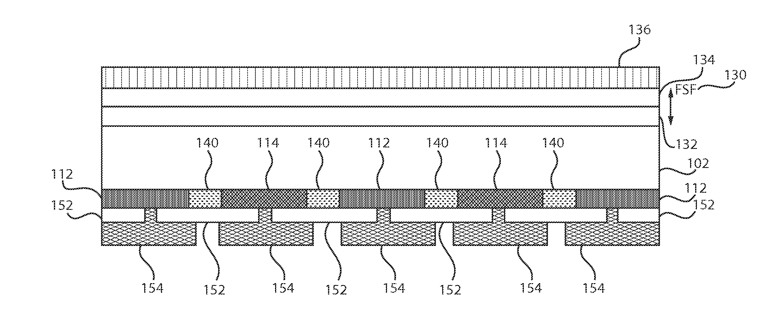
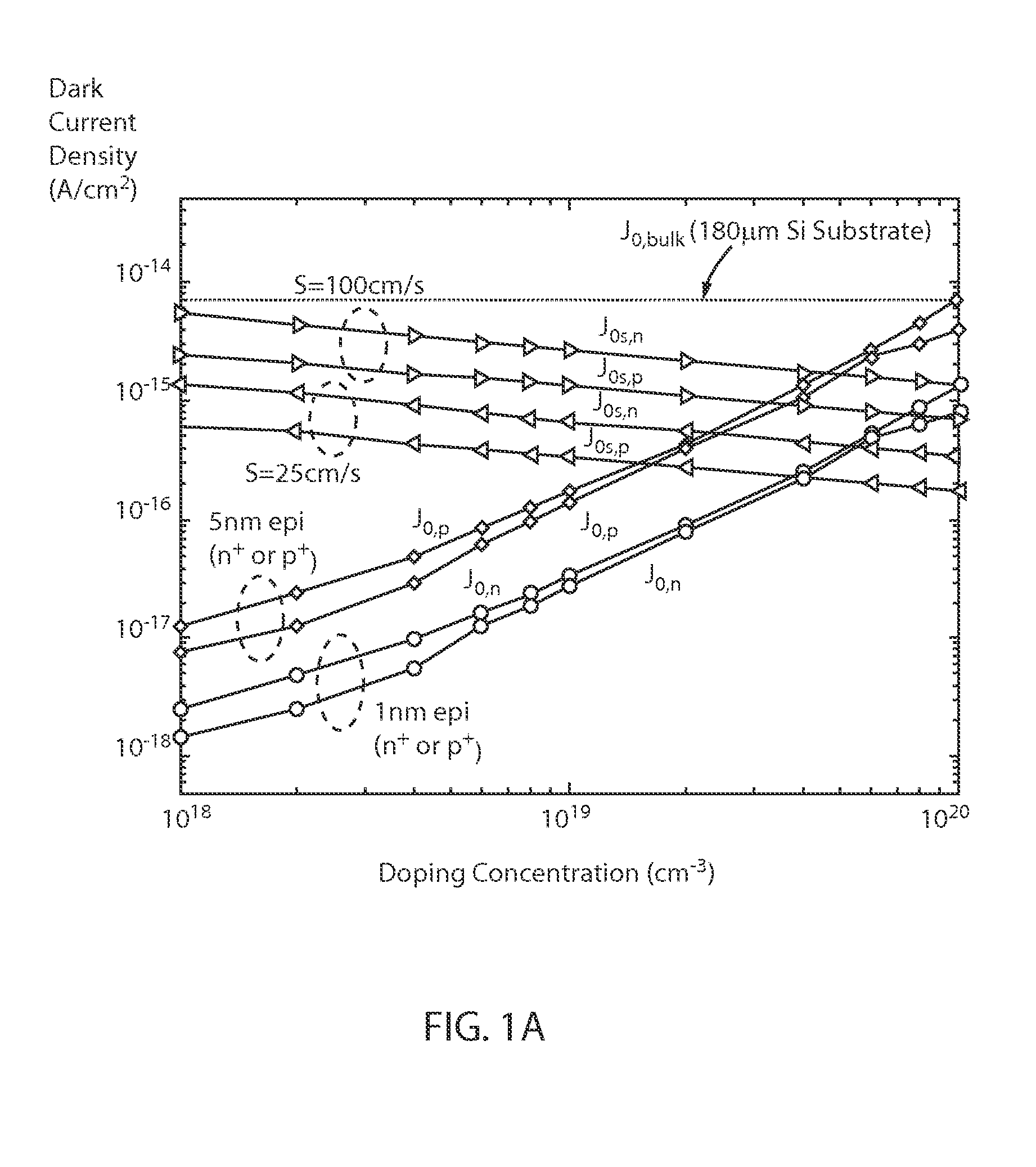
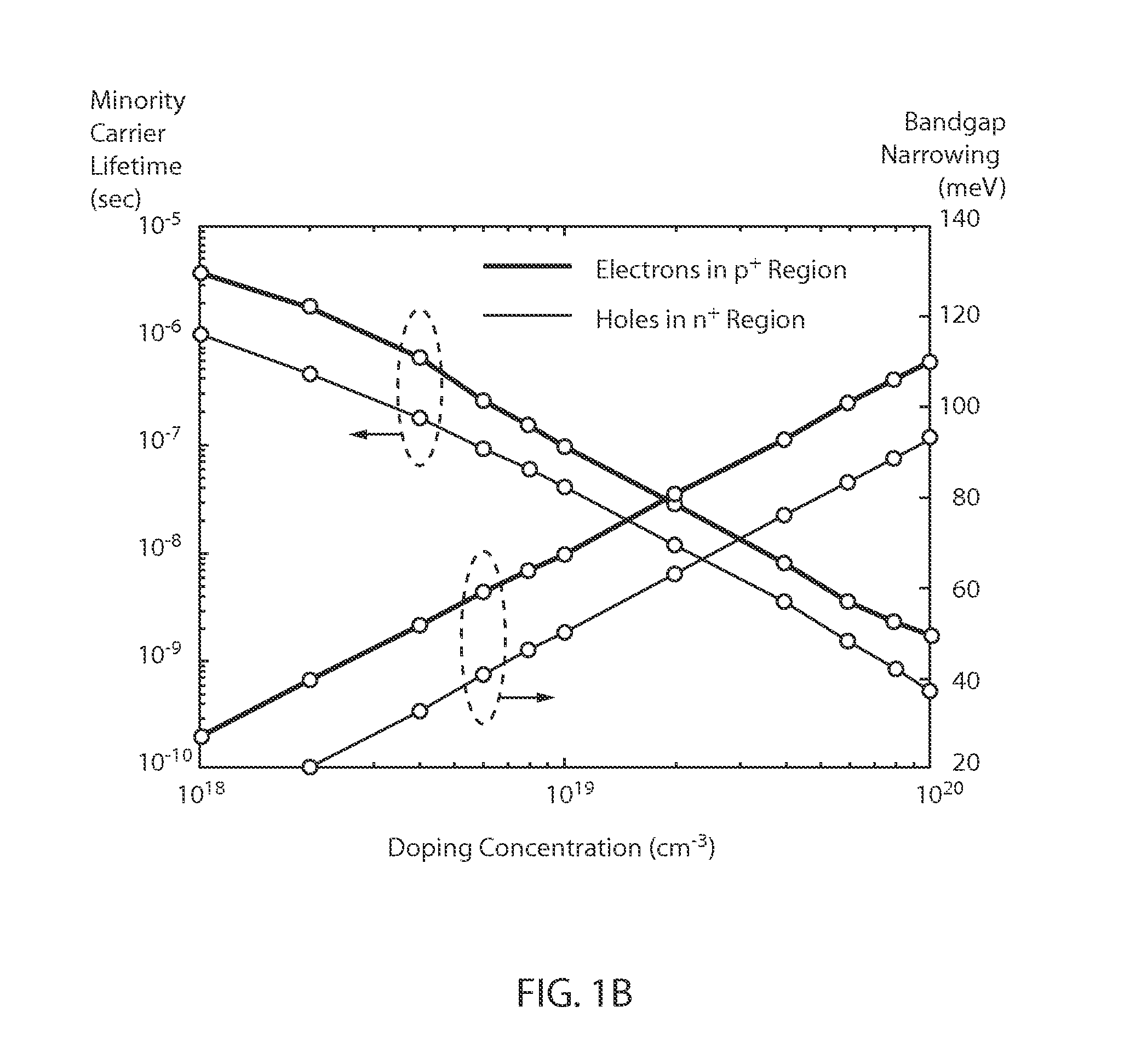
[0029]In accordance with the present principles, photovoltaic devices are provided having junctions formed that are thin (preferably less than about 5 nm), highly doped (preferably greater than 1019 cm−3) epitaxial (epi) layers with very low dislocation density (e.g., less than 105 cm−2) resulting in shallow junctions essentially having a depth equal to that of the epitaxial layer thickness. The very thin epitaxial layers result in low Auger recombination levels and have little or no impact on photovoltaic cell performance. In addition, due to the high doping concentration in the epi layer(s), a density of minority carriers reaching a substrate surface is reduced, and therefore a modest surface passivation is sufficient to achieve sufficiently low surface recombination levels. The thin epitaxial layers also permit short growth times, which is desirable for high manufacturing throughput.

[0030]In one embodiment, an interdigitated back-contact (IBC) photovoltaic device includes junctio...


PUM


Abstract

A method for fabricating a photovoltaic device includes forming a first contact on a crystalline substrate, by epitaxially growing a first doped layer having a doping concentration of 1019 cm−3 or greater, a dislocation density of 105 cm−2 or smaller, a hydrogen content of 0.1 atomic percent or smaller, and a thickness configured to reduce Auger recombination in the epitaxially grown doped layer. A first passivation layer is formed on the first doped layer. A second contact is formed on the crystalline substrate on a side opposite the first contact by epitaxially growing a second doped layer having a doping concentration of 1019 cm−3 or greater, a dislocation density of 105 cm−2 or smaller, a hydrogen content of 0.1 atomic percent or smaller and a thickness configured to reduce Auger recombination in the second epitaxially grown doped layer. A second passivation layer is formed on the second doped layer.

Description

RELATED APPLICATION DATA[0001]This application is a Continuation application of co-pending U.S. patent application Ser. No. 14 / 025,525 filed on Sep. 12, 2013, incorporated herein by reference in its entirety.BACKGROUND[0002]1. Technical Field[0003]The present invention relates to photovoltaic devices, and more particularly to devices and methods with passivated shallow junctions to reduce Auger recombination effects.[0004]2. Description of the Related Art[0005]In conventional front-contact solar cells, junctions are formed by diffusion and typically are a few hundreds of nanometers but less than 1 micron deep. Although higher doping levels are desired for increasing the splitting of quasi-Fermi levels and thus improving an open circuit voltage of the solar cell, the doping levels are chosen below 1019 cm−3 (typically the mid to upper 1018 cm−3 range) to avoid excessive Auger recombination in the highly doped region.[0006]In conventional interdigitated back-contact (IBC) solar cells,...

Claims


Application Information

Patent Timeline
IPC IPC(8): H01L31/0224
CPCH01L31/022441H01L31/068H01L31/0682H01L31/1804Y02E10/547H01L31/02167H01L31/022466Y02P70/50H01L31/18H01L31/0392
Inventor CHAN, KEVIN K.HEKMATSHOARTABARI, BAHMANNING, TAK H.
Owner GLOBALFOUNDRIES INC
Features
  • Generate Ideas
  • Intellectual Property
  • Life Sciences
  • Materials
  • Tech Scout
  • Unparalleled Data Quality
  • Higher Quality Content
  • 60% Fewer Hallucinations
Learn More